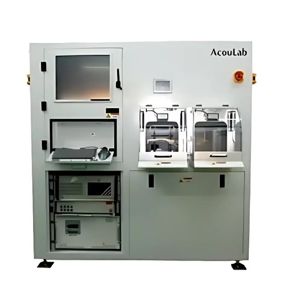
Acoulab SAM-CYGNUS Fully Automated Wafer Scanning Acoustic Microscope
| Brand | Acoulab |
|---|---|
| Origin | South Korea |
| Model | SAM-CYGNUS |
| Instrument Type | Digital |
| Wafer Compatibility | 4" and 6" |
| Ultrasonic Transducer Frequency Range | 1–500 MHz |
| A/D Sampling Rate | 2 GHz |
| Bandwidth | 1 GHz |
| XY Repeatability | ±2 µm |
| Z-Scan Range | 70 mm |
| Z-Resolution | 2.5 µm |
| Scan Modes | A-scan, C-scan, T-scan, X-scan (multi-layer C-scan) |
| Integrated Systems | Wafer Map module, BCR reader, Pre-aligner, Spin Coater, Water Jet Scanning, Safety Interlock & Alarm System |
| Motor Drive | High-precision linear servo motors |
| Acoustic Coupling | Water jet coupling |
Overview
The Acoulab SAM-CYGNUS is a fully automated scanning acoustic microscope (SAM) engineered for non-destructive evaluation of semiconductor wafers and LED substrates. It operates on the principle of high-frequency ultrasonic pulse-echo imaging, where broadband acoustic waves (1–500 MHz) are transmitted into the sample via water jet coupling; internal interfaces, discontinuities, and material property variations generate echo signals that are digitized at 2 GHz sampling rate with 1 GHz bandwidth. The system reconstructs subsurface features—including delamination, voids, cracks, interfacial debonding, and foreign inclusions—with micron-level spatial fidelity. Designed specifically for 4-inch and 6-inch wafers, the SAM-CYGNUS integrates precision motion control, real-time signal processing, and industrial-grade automation to support high-throughput metrology in wafer fabrication, packaging qualification, and failure analysis laboratories.
Key Features
- Fully automated workflow enabled by integrated robotic handler, wafer pre-aligner, BCR (Bar Code Reader), and wafer mapping software—eliminating manual loading and alignment errors.
- High-resolution XYZ motion system: dual-axis linear servo motors deliver ±2 µm repeatability in XY and 2.5 µm resolution in Z over a 70 mm vertical scan range.
- Water jet acoustic coupling ensures stable, low-noise transmission across diverse wafer topographies without physical contact or couplant residue.
- Multi-mode imaging capability: A-scan (time-domain waveform), C-scan (planar cross-section at selected depth), T-scan (through-thickness composite), and X-scan (layer-resolved C-scan stacks).
- Comprehensive safety architecture including hardware interlocks, emergency stop circuitry, audible/visual alarm triggers, and access-controlled operational zones compliant with IEC 61000-6-2/6-4 EMC standards.
- Low acoustic noise design achieved through vibration-damped linear servo actuation—critical for maintaining signal-to-noise ratio during long-duration scans.
Sample Compatibility & Compliance
The SAM-CYGNUS supports standard silicon, sapphire, GaN, and SiC wafers up to 150 mm (6″) in diameter, including patterned, thinned, bonded, and temporary-laminated substrates used in advanced packaging (e.g., TSV, fan-out, hybrid bonding). It accommodates both bare die and full-wafer formats with minimal setup time. All scanning protocols and data acquisition parameters adhere to ASTM E1742/E2983 for acoustic microscopy of microelectronic packages and ISO/IEC 17025 requirements for accredited testing laboratories. Optional audit trail logging and user-access controls align with FDA 21 CFR Part 11 and GLP/GMP documentation frameworks.
Software & Data Management
The proprietary Acoulab SAM Suite provides intuitive GUI-driven operation, real-time image reconstruction, and hierarchical data management. Users define inspection recipes—including ROI selection, depth gating, threshold-based defect classification, and automatic defect annotation—with version-controlled storage. Raw RF data (IQ format), processed C-scan images (TIFF, BMP), and measurement reports (PDF, CSV) are exportable with embedded metadata (timestamp, operator ID, calibration status, instrument configuration). The software supports batch processing, statistical process control (SPC) charting, and integration with MES/ERP systems via OPC UA or RESTful API. All data modifications are logged with immutable timestamps for traceability.
Applications
- Qualification of wafer-level bonding integrity in 3D IC and heterogeneous integration processes.
- Detection and sizing of sub-micron delamination at die-attach, underfill, and redistribution layer (RDL) interfaces.
- Void quantification in solder bumps, copper pillars, and electroplated metallization layers.
- Crack propagation analysis in brittle substrates (e.g., GaN-on-sapphire) following dicing, grinding, or thermal cycling.
- Thickness mapping of thin-film stacks and passivation layers using time-of-flight calculations from front- and back-surface echoes.
- Root cause analysis in LED manufacturing—identifying epoxy voids, phosphor layer separation, and substrate fracture prior to singulation.
FAQ
What wafer sizes does the SAM-CYGNUS support?
The system is configured for 4-inch (100 mm) and 6-inch (150 mm) wafers, with optional tooling kits available for handling smaller test coupons or diced dies.
Is water jet coupling mandatory?
Yes—the water jet delivery system is integral to achieving consistent acoustic impedance matching and eliminating air gaps; it also enables dynamic focus adjustment during Z-scans.
Can the SAM-CYGNUS perform quantitative thickness measurements?
Yes—using calibrated time-of-flight measurements from dual interface echoes, thickness accuracy is typically ±0.5% of measured value for homogeneous layers ≥5 µm thick.
Does the system comply with regulatory data integrity requirements?
When configured with audit trail, electronic signature, and role-based access modules, the SAM Suite meets FDA 21 CFR Part 11 and EU Annex 11 expectations for regulated environments.
What maintenance is required for long-term stability?
Routine calibration includes transducer frequency response verification, Z-stage encoder validation, and water purity monitoring; annual preventive maintenance is recommended per Acoulab’s service schedule.


