adphos PBT Ultrafast Near-Infrared (NIR) Sintering System
| Brand | adphos |
|---|---|
| Origin | Germany |
| Model | PBT |
| Technology | Ultrafast NIR Thermal Processing |
| Wavelength Range | 800–1200 nm |
| Peak Power Density | Up to 100 MW/ft² (focused line geometry) |
| Substrate Compatibility | PET, PI, PVC, Paper, Foils, Flexible Polymers |
| Process Speed | Up to 300 m/min |
| Operating Mode | Continuous web or batch |
| Compliance | CE, RoHS, ISO 9001-certified manufacturing |
Overview
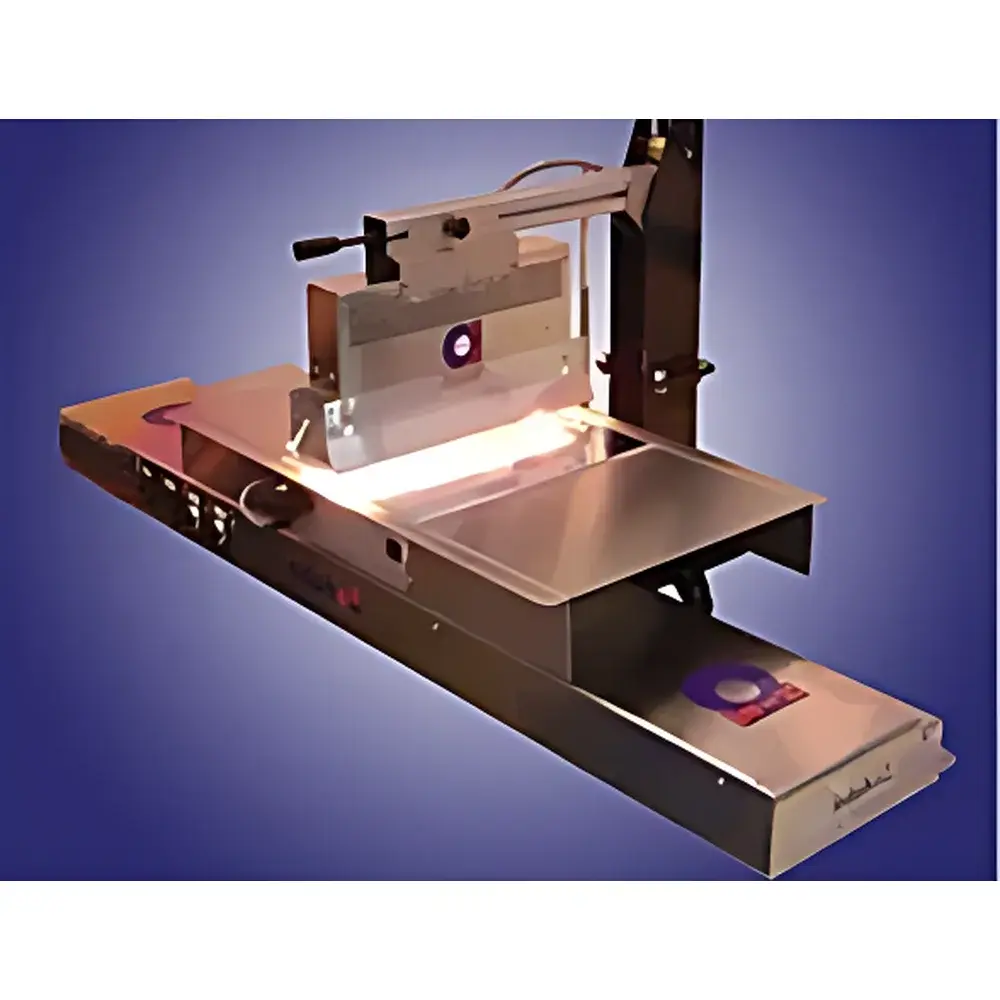
The adphos PBT Ultrafast Near-Infrared (NIR) Sintering System is an industrial-grade thermal processing platform engineered for high-speed, low-thermal-impact sintering and annealing of conductive inks on temperature-sensitive substrates. Unlike conventional IR, convection, or UV curing systems, the PBT leverages pulsed, spectrally optimized near-infrared radiation (800–1200 nm) to deliver energy directly into functional layers—bypassing substrate absorption and minimizing heat accumulation in the base material. This principle relies on selective photothermal coupling: most flexible polymeric substrates (e.g., PET, PI, PVC, paper) exhibit minimal absorption in the NIR band, while metallic or metal-oxide nanoparticles (Ag, Cu, Ni, ITO, ZnO) embedded in printed layers strongly absorb and convert NIR photons into localized thermal energy. As a result, full sintering occurs within seconds—even at web speeds up to 300 m/min—while substrate surface temperatures remain below critical thresholds (typically <80 °C for PET, <60 °C for paper), preserving dimensional stability and preventing warping, yellowing, or delamination.
Key Features
- Ultrafast NIR emitter array with microsecond-level pulse control and real-time power modulation
- Focused line geometry enabling peak power densities up to 100 MW/ft² for deep, uniform layer penetration
- Optimized spectral output centered at 1050 nm—maximizing ink absorption while minimizing substrate heating
- Integrated pyrometric feedback loop for closed-loop temperature monitoring of both coating and substrate surfaces
- Modular design supporting integration into roll-to-roll (R2R) printing lines, sheet-fed platforms, or standalone benchtop configurations
- Robust stainless-steel housing with IP54-rated enclosure and active cooling for continuous 24/7 operation
- No consumables, no ozone generation, no UV-induced degradation—fully compatible with organic semiconductors and perovskite precursors
Sample Compatibility & Compliance
The PBT system accommodates a broad range of printed electronic structures: silver nanoparticle inks, copper nanowire networks, carbon nanotube dispersions, PEDOT:PSS formulations, and metal-oxide nanoparticle pastes (e.g., ZnO, SnO₂). It supports substrates from 25 µm PET films to 300 g/m² coated paper, including laminated composites and metallized foils. All adphos systems are manufactured in Germany under ISO 9001 quality management protocols and comply with EU Machinery Directive 2006/42/EC, Electromagnetic Compatibility Directive 2014/30/EU, and RoHS 2011/65/EU. For regulated environments—including medical device manufacturing or automotive electronics qualification—the system architecture supports optional audit-ready data logging aligned with FDA 21 CFR Part 11 requirements when paired with validated software modules.
Software & Data Management
Control is executed via adphos’ proprietary NIR-OS™ interface—a deterministic real-time operating system running on an industrial PC with dual Ethernet ports (one for machine control, one for factory network integration). The GUI provides synchronized waveform visualization of irradiance profiles, temporal pulse sequencing, and multi-zone power mapping. All process parameters—including dwell time, peak irradiance, pulse repetition rate, and substrate speed—are logged with timestamped metadata and exportable in CSV or HDF5 format. Optional OPC UA server enables seamless integration with MES/SCADA platforms (Siemens SIMATIC, Rockwell FactoryTalk). Audit trails record user login events, parameter changes, and emergency stop activations—meeting GLP/GMP traceability expectations for R&D labs and pilot production facilities.
Applications
- Roll-to-roll sintering of Ag/Cu nanoparticle inks for RFID antennas, smart packaging sensors, and flexible PCB interconnects
- Low-temperature annealing of solution-processed oxide TFT backplanes on PEN substrates
- Curing of conductive polymer patterns without crosslinker decomposition or chain scission
- Thermal treatment of printed perovskite precursor layers prior to crystallization—avoiding solvent boiling artifacts
- Post-deposition densification of inkjet-printed transparent electrodes (ITO, AZO) on heat-labile bioplastics
- Functionalization of textile-integrated circuits where thermal mass constraints prohibit oven-based processing
FAQ
How does ultrafast NIR differ from conventional IR drying?
Conventional IR systems emit broadband radiation (1–10 µm), most of which is absorbed at the substrate surface—causing slow conductive heating through the layer stack. Ultrafast NIR uses narrowband, high-peak-power pulses at 800–1200 nm, enabling volumetric heating of the ink layer with minimal substrate interaction.
Can the PBT system be integrated into existing digital printing lines?
Yes—standardized mechanical interfaces (ISO 8502 flanges), EtherCAT motion synchronization, and configurable I/O modules allow plug-and-play integration with HP PageWide, Canon UVgel, or Xeikon CIJ platforms.
Is nitrogen purging required for oxygen-sensitive inks?
Not inherently—the PBT operates in ambient air; however, optional inline N₂ shrouds or glovebox-compatible enclosures are available for reactive metal inks (e.g., Cu nanoparticles).
What maintenance is required?
Annual calibration of radiometric sensors and inspection of quartz transmission windows; no lamp replacements or reflector recoating needed—solid-state emitters have >20,000 hours rated lifetime.
Does adphos provide application support for ink formulation optimization?
Yes—adphos maintains a global Application Development Lab offering joint DOE studies, thermal modeling (COMSOL Multiphysics®), and sintering protocol transfer for qualified ink suppliers (e.g., Heraeus, Sun Chemical, NanoMas).

")