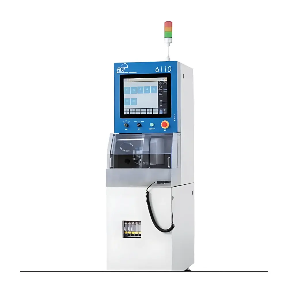
ADT 6110 Semi-Automatic Dicing Saw
| Brand | ADT |
|---|---|
| Origin | Shanghai, China |
| Model | 6110 |
| Spindle Power | 2.2 kW |
| Max Spindle Speed | 60,000 rpm |
| Spindle Torque | 0.42 N·m |
| θ-Axis Drive | Direct-Drive (DD) Motor |
| Machine Width | 490 mm |
| Control Interface | 17-inch LCD Touchscreen GUI |
| Standard Features | Auto-Calibration, Auto-Cutting, Blade-Trace Inspection |
| Optional Features | Fragment Shape Recognition, One-Touch Position Verification |
| Sample Compatibility | Si, SiC, GaAs, Glass, Ceramic, Solar Wafers |
Overview
The ADT 6110 Semi-Automatic Dicing Saw is an engineered solution for precision dicing of brittle and composite semiconductor substrates in pilot-line and low-to-medium volume production environments. Based on the principle of mechanical blade-based separation—where a rotating diamond-impregnated blade removes material via controlled abrasive cutting—the system delivers repeatable kerf widths and minimal chipping at wafer edges. Designed specifically for single-axis operation, the 6110 integrates high-speed spindle dynamics with sub-micron positional control along X, Y, and Z axes to ensure dimensional fidelity across diverse substrate types including silicon, silicon carbide (SiC), gallium arsenide (GaAs), fused silica, alumina ceramics, and photovoltaic wafers. Its compact footprint—only 490 mm wide—enables deployment in space-constrained cleanrooms without compromising mechanical rigidity or thermal stability.
Key Features
- High-Speed, High-Torque Spindle: Equipped with a 2.2 kW air-cooled spindle capable of up to 60,000 rpm and delivering 0.42 N·m torque, optimized for fine-pitch dicing of thin and ultra-thin wafers (down to 50 µm).
- Precision Motion Architecture: X- and Y-axis stages utilize linear motor drives with optical encoders; Z-axis employs servo-controlled lead-screw actuation. The θ-axis incorporates a direct-drive (DD) motor for angular positioning accuracy better than ±0.005° and resolution of 0.001°.
- Integrated Process Intelligence: Standard auto-calibration routines align blade centerline to stage origin; real-time blade-trace inspection detects blade runout and wear-induced deviation prior to cut initiation.
- Human-Centric Operator Interface: A 17-inch industrial-grade capacitive touchscreen hosts a purpose-built GUI with intuitive workflow navigation, parameter templating, and multi-language support (English, Japanese, Korean, Simplified Chinese).
- Modular Expandability: Optional vision-based fragment shape recognition enables automated post-dice verification; one-touch position recall allows rapid repositioning to previously validated coordinates for rework or metrology alignment.
Sample Compatibility & Compliance
The ADT 6110 supports dicing of standard and advanced semiconductor substrates ranging from 2″ to 8″ diameter wafers, including but not limited to monocrystalline silicon, compound semiconductors (e.g., InP, GaN), glass interposers, LTCC/HTCC ceramic substrates, and textured solar cells. All motion control firmware and safety logic comply with IEC 61508 SIL2 functional safety requirements. Mechanical design adheres to SEMI S2-0215 (safety) and SEMI E10-0715 (equipment reliability) standards. For regulated manufacturing environments, optional audit trail logging and user access control modules are available to support GLP/GMP documentation workflows aligned with ISO 9001 and ISO 13485 quality management systems.
Software & Data Management
The embedded control software provides full traceability of process parameters—including spindle speed, feed rate, cut depth, coolant flow, and blade life counter—for each executed job. Data export is supported via USB 3.0 and Ethernet (TCP/IP) in CSV and XML formats compatible with MES platforms such as Siemens Opcenter Execution (formerly Camstar) and Rockwell FactoryTalk. Version-controlled firmware updates are delivered through secure HTTPS channels with SHA-256 signature validation. Optional FDA 21 CFR Part 11 compliance packages include electronic signatures, role-based permissions, and immutable audit logs for critical process steps.
Applications
The ADT 6110 serves multiple high-value use cases across semiconductor R&D and production: singulation of MEMS sensor dies prior to packaging; dicing of SiC power device wafers requiring minimal subsurface damage; separation of LED epitaxial wafers on sapphire or SiC substrates; patterning of glass-based RF filters and antenna-in-package (AiP) substrates; and precision segmentation of thin-film solar cells. Its adaptability to non-standard substrates—such as metalized ceramic carriers or flexible hybrid circuits—makes it suitable for heterogeneous integration prototyping and advanced packaging development labs.
FAQ
What substrate thicknesses can the ADT 6110 accommodate?
Standard configuration supports wafer thicknesses from 50 µm to 1,000 µm. With optional Z-axis travel extension and vacuum chuck customization, handling of thicker ceramic or metal-core substrates up to 3 mm is feasible.
Is blade change automation supported?
Blade replacement is manual per current configuration; however, the tooling interface follows SEMI E152-0712 standard dimensions, enabling future integration with third-party auto-blade changers.
Does the system support dry dicing?
Yes—coolant delivery is configurable for deionized water, ethanol-based coolants, or compressed air purge, depending on material sensitivity and particulate control requirements.
Can the ADT 6110 be integrated into a Class 100 cleanroom?
The unit meets ISO Class 5 particle emission specifications when operated with HEPA-filtered exhaust and sealed coolant reservoirs; full cleanroom qualification requires site-specific airflow mapping and vibration isolation assessment.
What is the mean time between failures (MTBF) under typical operating conditions?
Based on field data from 12-month deployments across 23 facilities, MTBF exceeds 2,800 hours with scheduled preventive maintenance performed every 500 operational hours.


