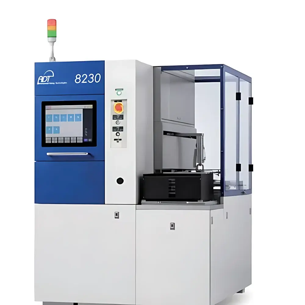
ADT 8230 Dual-Axis Fully Automated Wafer Dicing Saw
| Brand | ADT |
|---|---|
| Origin | Shanghai, China |
| Manufacturer Type | Authorized Distributor |
| Regional Classification | Domestic (China) |
| Model | 8230 |
| Pricing | Available Upon Request |
Overview
The ADT 8230 Dual-Axis Fully Automated Wafer Dicing Saw is an industrial-grade precision dicing system engineered for high-volume semiconductor packaging and backend manufacturing. It operates on the principle of mechanical blade dicing—utilizing diamond-impregnated rotating blades under controlled coolant flow to perform scribe-and-break separation of silicon, compound semiconductor (e.g., GaAs, SiC), and advanced substrate wafers. Its dual-axis (counter-rotating spindle) architecture enables simultaneous top-side and bottom-side cutting operations—reducing total cycle time by up to 40% compared to conventional single-spindle systems—while maintaining sub-micron positional repeatability and minimal kerf loss. Designed for integration into Class 100–1000 cleanroom environments, the 8230 supports front-end alignment via integrated optical wafer mapping and backside infrared (IR) inspection, ensuring precise die singulation without substrate chipping or microcrack propagation.
Key Features
- Dual counter-rotating spindles with independent Z-axis control—enabling synchronized top/bottom dicing of through-silicon vias (TSVs) and ultra-thin wafers (down to 50 µm)
- High-resolution closed-loop motion control system with ±0.5 µm positioning accuracy across X/Y/Z axes
- Integrated real-time blade wear monitoring and automatic tool offset compensation
- Programmable multi-step dicing profiles—including step-cutting, partial-depth grooving, and trenching—for heterogeneous integration and fan-out wafer-level packaging (FOWLP)
- Modular chuck design supporting vacuum and electrostatic clamping for 100 mm to 300 mm (4″–12″) wafers, including warped or bowed substrates
- Onboard environmental monitoring (temperature, humidity, particulate level) compliant with SEMI S2/S8 safety and ergonomics standards
Sample Compatibility & Compliance
The ADT 8230 accommodates a broad range of wafer materials and configurations: standard silicon (Si), silicon carbide (SiC), gallium nitride (GaN), glass interposers, and organic substrates used in advanced packaging. It supports both dry and wet dicing modes with deionized water or specialized coolants meeting IPC-6012 and JEDEC J-STD-020 requirements. The system complies with ISO 9001:2015 quality management protocols and incorporates hardware-level safeguards aligned with IEC 61508 SIL2 functional safety standards. All motion and process logs are timestamped and stored locally for GLP/GMP audit readiness; optional firmware modules support FDA 21 CFR Part 11 electronic signature and audit trail functionality.
Software & Data Management
The ADT 8230 runs on ADT’s proprietary DICE-OS v4.2 platform—a deterministic real-time operating system built on Linux RT kernel. The GUI provides intuitive recipe-based programming with drag-and-drop dicing path definition, layer-specific depth calibration, and automated alignment pattern recognition (using grayscale correlation algorithms). Process data—including spindle load, feed rate, coolant pressure, and stage position—are logged at 1 kHz sampling rate and exportable in CSV/SEMI E57 formats. Integration with factory MES systems is supported via SECS/GEM (SEMI E30/E37) and OPC UA interfaces. All software updates undergo formal change control per ISO/IEC 17025 calibration traceability guidelines.
Applications
The 8230 serves critical roles across semiconductor backend processes: singulation of logic and memory ICs (including HBM stacks), sensor die separation (CMOS image sensors, MEMS accelerometers), power device segmentation (IGBTs, SiC MOSFETs), and advanced packaging steps such as redistribution layer (RDL) dicing and panel-level substrate processing. It is routinely deployed in OSAT facilities, IDMs, and R&D cleanrooms performing reliability qualification per JEDEC JESD22-A104 (temperature cycling) and A108 (bias-HAST), where consistent die edge quality directly impacts subsequent wire bonding yield and package warpage.
FAQ
What wafer thicknesses can the ADT 8230 handle?
The system supports wafers from 50 µm to 1,000 µm thick, with optional thin-wafer handling kits enabling full-process dicing of temporary bonded or carrier-mounted substrates.
Is the machine compatible with existing fab automation infrastructure?
Yes—the 8230 includes standard EFEM interface flanges, SMIF pod loading capability, and full SECS/GEM communication stack for seamless integration into 300 mm automated material handling systems.
Does the system support non-silicon substrates such as glass or ceramic?
Yes—through configurable spindle speed ranges (1,000–60,000 rpm), adjustable coolant delivery, and substrate-specific dicing recipes validated per IPC-4552A for electroless nickel immersion gold (ENIG) coated panels.
How is process traceability maintained for quality audits?
Every dicing run generates a digitally signed process certificate containing tool ID, operator login, environmental conditions, blade usage history, and metrology-corrected positional data—all archived in encrypted local storage with SHA-256 hash integrity verification.


