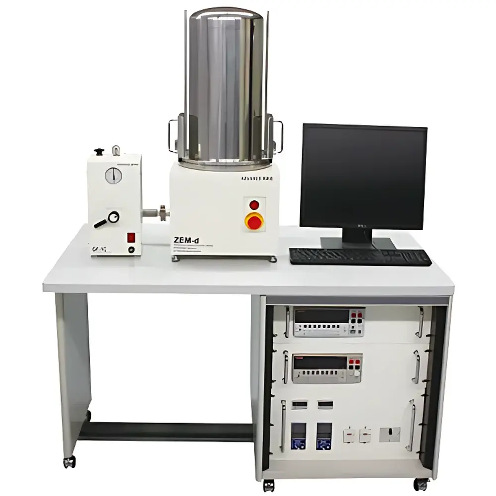
ADVANCE RIKO ZEM-d Polymer Thin-Film Through-Thickness Thermoelectric Property Evaluation System
| Brand | ADVANCE RIKO |
|---|---|
| Origin | Japan |
| Model | ZEM-d |
| Temperature Range | Up to 200 °C (sample surface) |
| Sample Cross-Section | Ø20 mm (max) |
| Sample Thickness | 10 µm – 20 mm |
| Measured Properties | Seebeck coefficient (S), electrical resistivity (ρ) |
| Atmosphere | Air or inert gas (N₂, Ar) |
| Measurement Orientation | Through-thickness (z-direction) |
Overview
The ADVANCE RIKO ZEM-d is a purpose-built thermoelectric property evaluation system engineered for precise, contact-based measurement of the Seebeck coefficient (S) and electrical resistivity (ρ) in polymer thin films along the through-thickness (z-) direction. Unlike conventional in-plane thermoelectric characterization platforms such as the ZEM-3 or ZEM-5, the ZEM-d addresses a critical metrological gap in soft-material thermoelectrics: the quantification of anisotropic transport properties perpendicular to the film plane—where charge and heat carriers experience distinct interfacial, morphological, and phonon-scattering environments. Its design adheres to the principles of steady-state, two-probe DC electrical and differential thermoelectric voltage measurement under controlled thermal gradient conditions. The system applies a calibrated, symmetric temperature gradient across the film thickness while simultaneously recording voltage and current responses with nanovolt-level resolution and sub-microampere current control. This architecture enables direct determination of S and ρ without geometric correction assumptions commonly required in lateral configurations—particularly advantageous for low-conductivity, high-resistivity polymer systems where contact resistance and edge effects dominate.
Key Features
- Through-thickness (z-axis) measurement capability optimized for freestanding or substrate-supported polymer films as thin as 10 µm
- Integrated dual-thermocouple sensor array for accurate, localized thermal gradient monitoring at both film interfaces
- High-stability DC current source (0.1 µA–10 mA range) with programmable ramping and compliance limits
- Low-noise nanovoltmeter (±100 nV resolution) synchronized with temperature acquisition for simultaneous S and ρ calculation
- Heated sample stage with PID-controlled temperature regulation up to 200 °C (surface reading), ensuring reproducible thermal boundary conditions
- Sealed chamber compatible with ambient air or inert atmospheres (N₂, Ar) to prevent oxidative degradation during elevated-temperature testing
- Modular electrode fixture accommodating circular samples up to Ø20 mm with adjustable pressure control to minimize contact resistance variability
Sample Compatibility & Compliance
The ZEM-d supports a broad class of thermally and electrically heterogeneous polymeric systems—including conjugated polymers (e.g., PEDOT:PSS derivatives), ion-conducting elastomers, block copolymer nanocomposites, and layered organic-inorganic hybrids. Its mechanical fixture accommodates both rigid freestanding films and flexible substrates (e.g., PET, PI, glass) with minimal clamping-induced strain. All measurement protocols are traceable to SI units via NIST-traceable calibration standards for voltage, current, and temperature. While not certified to a specific ISO standard, the system’s architecture and data acquisition logic align with ASTM D926 (Standard Test Method for Electrical Resistivity of Solid Electrical Insulating Materials) and ASTM E2981 (Standard Guide for Thermoelectric Property Measurements), and its software audit trail functionality supports GLP-compliant documentation requirements per FDA 21 CFR Part 11 when configured with user access controls and electronic signature modules.
Software & Data Management
The proprietary ZEM-d Control & Analysis Suite provides real-time visualization of ΔT, VSeebeck, I, and calculated S and ρ values during each temperature step. Data files are exported in ASCII-compatible .csv format with metadata headers including timestamp, setpoint temperature, ambient gas, and operator ID. The software implements automatic baseline drift correction using open-circuit reference measurements before each thermal ramp. Batch processing tools enable comparative analysis across multiple samples or thermal cycles, with built-in uncertainty propagation based on instrument specifications and sample geometry tolerances. Raw voltage and temperature logs are stored with millisecond time stamps, facilitating post-hoc validation of thermal equilibrium criteria (e.g., dT/dt < 0.01 °C/min over 60 s). Exported datasets conform to MIAME/MINSEQE metadata conventions for integration into institutional research data management (RDM) systems.
Applications
- Quantitative structure–property mapping of side-chain engineering effects on through-thickness charge transport in doped polyanilines
- Evaluation of interfacial thermal boundary resistance (Kapitza resistance) contributions to total thermal conductivity in multilayer polymer thermoelectrics
- In situ aging studies of thermoelectric performance degradation under thermal cycling (25–150 °C) in humidified or dry inert atmospheres
- Correlation of z-direction S and ρ with cross-plane thermal diffusivity (measured via laser flash analysis) to compute full-figure-of-merit (zT) profiles
- Process optimization feedback for roll-to-roll printed thermoelectric films, linking coating parameters to anisotropic transport metrics
- Validation of multiscale modeling outputs (e.g., Boltzmann transport + molecular dynamics simulations) for phonon-electron decoupling in amorphous organic semiconductors
FAQ
Can the ZEM-d measure absolute thermal conductivity?
No. The ZEM-d measures only Seebeck coefficient and electrical resistivity. Thermal conductivity must be determined separately—typically via laser flash analysis (LFA) or time-domain thermoreflectance (TDTR)—and combined with ZEM-d data to calculate zT.
Is substrate removal required for supported films?
Not necessarily. The system allows measurement of films on insulating substrates (e.g., quartz, sapphire) provided the substrate thickness is ≤10% of total stack thickness and its thermal expansion coefficient closely matches that of the film to avoid delamination-induced artifacts.
What is the minimum recommended contact area for reliable z-direction measurement?
A minimum effective contact area of 30 mm² is advised to ensure uniform current distribution and mitigate edge-current crowding; this corresponds to ~Ø6.2 mm for circular electrodes.
Does the system support automated multi-sample sequencing?
Yes—optional robotic sample loader integration enables unattended sequential measurement of up to 12 pre-aligned samples per run, with auto-calibration between batches.
How is thermal gradient linearity verified during operation?
The system performs real-time linear regression on thermocouple pair outputs at each temperature step; deviation >2% from linearity triggers an alert and pauses measurement until user intervention or recalibration.

")

