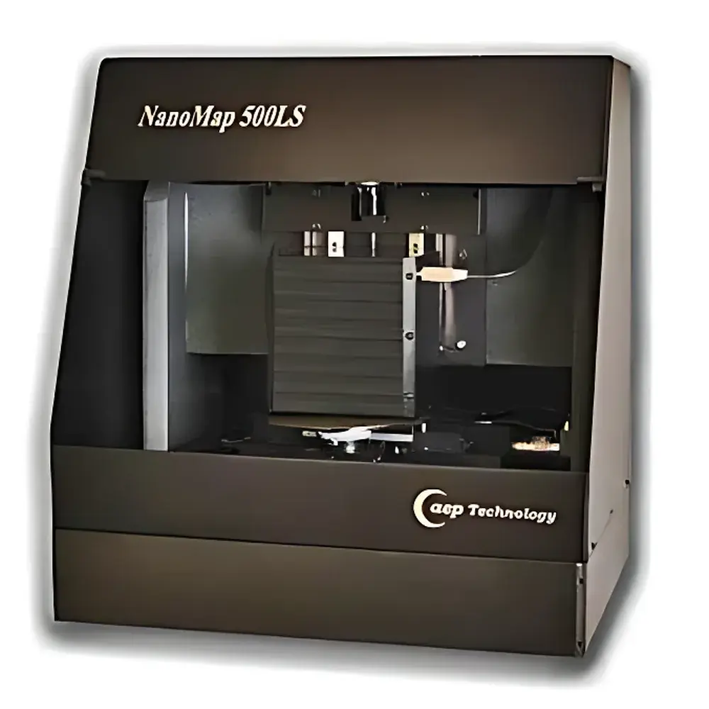
AEP Technology NANOMAP 500LS Contact Mode Profilometer & 3D Surface Topography Analyzer
| Brand | AEP Technology |
|---|---|
| Origin | USA |
| Model | NANOMAP 500LS |
| Type | Contact-mode profilometer / surface roughness analyzer |
| Vertical Resolution | ≤0.1 nm |
| Lateral Scan Range (Tip Scan) | 10 µm × 10 µm to 500 µm × 500 µm |
| Lateral Scan Range (Stage Scan) | up to 50 mm |
| Maximum Vertical Dynamic Range | 500 µm |
| Measurement Speed | High-speed scanning from 1 nm to 10 mm profiles |
| Sample Handling | No specialized preparation required |
Overview
The AEP Technology NANOMAP 500LS is a dual-mode contact profilometer engineered for high-precision, quantitative 3D surface topography analysis across micro- to macro-scale length regimes. It integrates the nanoscale resolution of scanning probe microscopy (SPM) with the large-field capability of precision mechanical stage profiling—enabling seamless transition between localized atomic-force-level characterization and extended-area industrial metrology. The system operates on the principle of mechanical tip-based surface tracing, where a diamond-tipped stylus maintains controlled, constant-force contact while traversing the sample surface. Vertical displacement is detected via dual optical interferometric sensors, delivering sub-nanometer vertical resolution (≤0.1 nm) and a dynamic range of up to 500 µm—critical for measuring steep slopes, deep trenches, or multilayer step heights without mode switching or sensor recalibration. Its hybrid architecture—combining piezoelectric tip scanning (10–500 µm range) with motorized optical-stage translation (up to 50 mm)—ensures traceable, reproducible measurements compliant with ISO 25178 (Geometrical Product Specifications – Surface texture) and ASTM E2941 (Standard Guide for Measuring Surface Roughness Using Contact Profilometers).
Key Features
- Dual-scanning architecture: Independent piezoelectric tip scanning (for high-resolution local mapping) and high-stability optical-stage scanning (for long-range, low-drift profiling)
- Constant-force feedback control: Software-regulated contact force ensures minimal sample deformation—even on soft polymers, thin films, or biological specimens
- Real-time optical visualization: Integrated color CCD camera enables precise tip positioning and in-situ feature identification during scan setup and navigation
- Simultaneous multi-parameter acquisition: Simultaneously records height, slope, curvature, area, volume, and statistical roughness parameters (Sa, Sq, Sz, Sdr, etc.) per scan
- Traceable calibration: Factory-certified reference standards included for vertical (step height) and lateral (pitch, linearity) verification per ISO/IEC 17025 guidelines
- Robust mechanical design: Granite base, air-isolated optical table integration, and thermal drift compensation ensure measurement stability over extended acquisition times
Sample Compatibility & Compliance
The NANOMAP 500LS accommodates diverse material classes without surface metallization or conductive coating—including dielectric thin films, sputtered coatings, polished optics, rolled metal sheets, paper substrates, ceramic wafers, MEMS devices, and hydrated biomaterials. Its non-destructive, low-force operation (adjustable from 10 µN to 5 mN) preserves surface integrity during repeated measurements. The instrument meets requirements for regulated environments: raw data files include embedded audit trails (user ID, timestamp, parameter settings), support GLP/GMP documentation workflows, and comply with FDA 21 CFR Part 11 when deployed with validated software configurations. All roughness calculations adhere to ISO 4287, ISO 4288, and ISO 25178-2 definitions; critical dimension reporting supports semiconductor industry standards including SEMI MF1526 and JEDEC JESD22-A108.
Software & Data Management
Acquisition and analysis are performed using AEP’s proprietary Nanomap™ v6.x software suite, built on a modular, scriptable platform compatible with Windows 10/11 (64-bit). The interface features intuitive two-step workflow navigation—first defining scan area and force parameters, then executing and reviewing results. Advanced modules enable cross-sectional extraction, grain boundary detection, film thickness deconvolution from step edges, wear volume quantification via 3D surface subtraction, and automated defect flagging based on user-defined height/slope thresholds. Data export supports ASCII, CSV, Metrology XML (ISO 10360-compliant), and common image formats (TIFF, BMP, PNG) with embedded metadata. Software validation packages—including IQ/OQ documentation templates and electronic signature support—are available for pharmaceutical, aerospace, and semiconductor QA/QC laboratories.
Applications
- Quantitative 3D surface texture analysis of optical lenses, laser mirrors, and EUV mask blanks
- Thin-film and multilayer step-height metrology in semiconductor fabrication (e.g., SiO₂/SiNₓ etch depth, photoresist profile)
- Wear track volumetric loss assessment in tribological testing of bearings, seals, and biomedical implants
- Surface flatness and curvature evaluation of precision-ground mechanical components per ASME B46.1
- MEMS device release inspection: stiction assessment, actuator deflection mapping, and comb-drive gap uniformity
- Coating delamination and blister quantification in automotive and aerospace protective layers
- Two-dimensional stress mapping via wafer bow analysis using sequential front/back surface topography
FAQ
What is the difference between tip scanning and stage scanning modes?
Tip scanning uses piezoelectric actuators for high-resolution, small-area mapping (≤500 µm); stage scanning employs a motorized, optically referenced platform for repeatable, low-drift profiling over distances up to 50 mm.
Can the NANOMAP 500LS measure transparent or highly reflective surfaces?
Yes—unlike optical interferometers, its contact-mode operation is insensitive to surface reflectivity, refractive index, or transparency, making it suitable for glass, quartz, sapphire, and polymer films.
Is calibration traceable to NIST standards?
All factory calibrations are performed using NIST-traceable step-height and line-spacing reference artifacts; calibration certificates include uncertainty budgets per ISO/IEC 17025.
Does the system support automated batch measurement?
Yes—the software supports programmable multi-site measurement routines with stage auto-positioning, conditional pass/fail logic, and report generation in PDF or Excel format.
What maintenance is required for long-term accuracy?
Annual verification using certified reference standards is recommended; stylus replacement intervals depend on usage but typically exceed 500 hours of active scanning under standard force conditions.