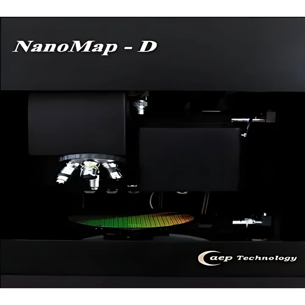
AEP Technology NANOMAP D Dual-Mode Optical-Probe Profilometer / 3D Surface Topography Metrology System
| Brand | AEP Technology |
|---|---|
| Origin | USA |
| Manufacturer Type | Authorized Distributor |
| Product Category | Imported Instrument |
| Model | NANOMAP D |
| Price Range | USD 65,000 – 130,000 |
| Type | Non-contact + Contact Hybrid Profilometer / Surface Roughness & 3D Topography Analyzer |
Overview
The AEP Technology NANOMAP D is a dual-mode surface metrology platform engineered for high-fidelity, quantitative 3D topographic characterization across micro- to macro-scale features. It uniquely integrates two complementary measurement principles—white-light interferometry (WLI) for rapid, non-contact, large-field-of-view profiling and scanning probe microscopy (SPM)-based contact mode for localized, sub-nanometer vertical resolution imaging—within a single, co-registered mechanical stage and software environment. This hybrid architecture addresses fundamental limitations inherent in standalone optical or probe-based systems: WLI provides speed, lateral scalability (up to 10 mm scan range), and immunity to tip convolution artifacts; SPM delivers atomic-scale vertical sensitivity (≤0.05 nm RMS noise), direct force-controlled surface interaction, and true nanoscale spatial fidelity on steep slopes and discontinuous topographies. The system is calibrated traceably to NIST-traceable standards, supporting ISO 25178-2 (areal surface texture), ISO 4287 (profile roughness), and ASTM E2921 (standard guide for 3D surface topography measurements), making it suitable for GLP/GMP-compliant R&D, process development, and quality assurance workflows in advanced manufacturing environments.
Key Features
- Dual-sensor fusion architecture: Simultaneous or sequential operation of white-light interferometry and SPM-based stylus/contact scanning on a shared XY-Z precision stage.
- NIST-traceable calibration: Integrated reference standards certified by the National Institute of Standards and Technology for vertical (step height), lateral (pitch), and roughness verification.
- Seamless stitching algorithm: Automated m×n image tiling with sub-pixel registration, enabling high-resolution (>1 nm lateral sampling) mapping over fields exceeding 10 mm × 10 mm without loss of metrological integrity.
- Vertical resolution: ≤0.05 nm RMS in SPM mode; ≤0.1 nm in WLI mode (with phase-shifting enhancement).
- Dynamic range: 1 nm to 10 mm vertical profile depth; lateral scan range up to 100 mm × 100 mm via motorized stage expansion option.
- No sample preparation required: Compatible with conductive, insulating, transparent, reflective, and fragile surfaces—including uncoated wafers, polymer films, biological substrates, and MEMS devices.
Sample Compatibility & Compliance
The NANOMAP D accommodates diverse material classes without metallization or vacuum requirements: semiconductor wafers (Si, GaN, SiC), optical coatings (AR/HR multilayers), thin-film photovoltaics (CIGS, perovskite), magnetic recording media, ceramic thermal barriers, paper and packaging substrates, and soft biomaterials (hydrogels, tissue scaffolds). Its measurement protocols comply with ISO 25178 series for areal surface texture parameters (Sa, Sq, Sz, Sk, Spk, Svk), ISO 4288 for profile-based roughness (Ra, Rz, Rq), and ASTM E2921 for uncertainty estimation in 3D topography. For regulated industries, the software supports audit trail logging, electronic signatures, and 21 CFR Part 11–compliant data handling when configured with optional validation packages.
Software & Data Management
The proprietary NanoMap Analysis Suite provides modular, scriptable analysis workflows covering 2D line profiles, 3D surface rendering, spectral analysis (PSD), curvature mapping, volume/area quantification (e.g., pit depth, coating thickness, wear volume), step-height metrology, and film stress calculation via Stoney’s equation. Advanced filtering includes Fourier-based high-pass, low-pass, band-pass, and notch filters; polynomial flattening; mask-based region-of-interest (ROI) definition; and adaptive interpolation. All raw and processed data are stored in vendor-neutral HDF5 format with embedded metadata (timestamp, operator ID, calibration status, environmental conditions). Batch processing, automated report generation (PDF/Excel), and API access (Python/C++) enable integration into automated FA labs and MES environments.
Applications
- Semiconductor process control: Trench depth, gate oxide uniformity, CMP endpoint detection, lithography resist profile analysis (including sub-100 nm feature sidewall angles).
- MEMS/MOEMS development: Mirror flatness, actuator displacement hysteresis, comb-drive gap uniformity, and stiction evaluation under controlled load.
- Optical component metrology: Surface figure error (PV, RMS), scratch/dig assessment, coating thickness on curved substrates, and diffractive optical element (DOE) fidelity.
- Thin-film and coating R&D: Stress-induced curvature, delamination onset detection, porosity quantification, and interfacial roughness evolution during deposition/annealing.
- Biomedical device characterization: Scaffold pore architecture, hydrogel swelling kinetics, and micro-patterned surface topography influencing cell adhesion.
FAQ
Does the NANOMAP D require vacuum or conductive coating for non-conductive samples?
No. Both WLI and contact SPM modes operate in ambient air without vacuum or sputter-coating, preserving native surface chemistry and morphology.
Can the system measure transparent thin films on silicon or glass substrates?
Yes. WLI mode resolves film thickness (down to ~10 nm) and interface roughness via interference fringe contrast analysis, independent of substrate opacity.
Is the software compliant with FDA 21 CFR Part 11 for regulated pharmaceutical or medical device applications?
Yes—when deployed with the validated software package and associated procedural controls (SOPs, change management, audit trail configuration), it meets ALCOA+ data integrity principles and Part 11 technical requirements.
What is the typical measurement uncertainty for step height calibration using NIST-traceable standards?
For steps between 10 nm and 1 µm, expanded uncertainty (k=2) is ≤1.2% of measured value, verified per ISO/IEC 17025-accredited calibration procedures.
How does the stitching algorithm maintain metrological accuracy across tiled images?
It employs cross-correlation-based sub-pixel alignment, distortion correction via stage encoder feedback, and overlap-based uncertainty weighting—ensuring <0.5 nm vertical consistency across stitched boundaries.