AET Coaxial Resonant Cavity Dielectric Constant Analyzer
| Brand | AET |
|---|---|
| Origin | Japan |
| Model | Coaxial Resonant Cavity System |
| Frequency Range | 800 MHz – 9.4 GHz |
| Permittivity (ε′) | 1–15 |
| Accuracy | ±1% |
| Loss Tangent (tan δ) | 0.001–0.1 |
| Accuracy | ±5% |
| Resonant Modes | Type A (0.8 / 2.45 / 4.2 / 5.8 / 7.6 GHz) and Type B (1.0 / 3.1 / 5.2 / 7.3 / 9.4 GHz) |
| Measurement Principle | High-Q coaxial cavity resonance with 3D electromagnetic field simulation (CST Microwave Studio®) |
Overview
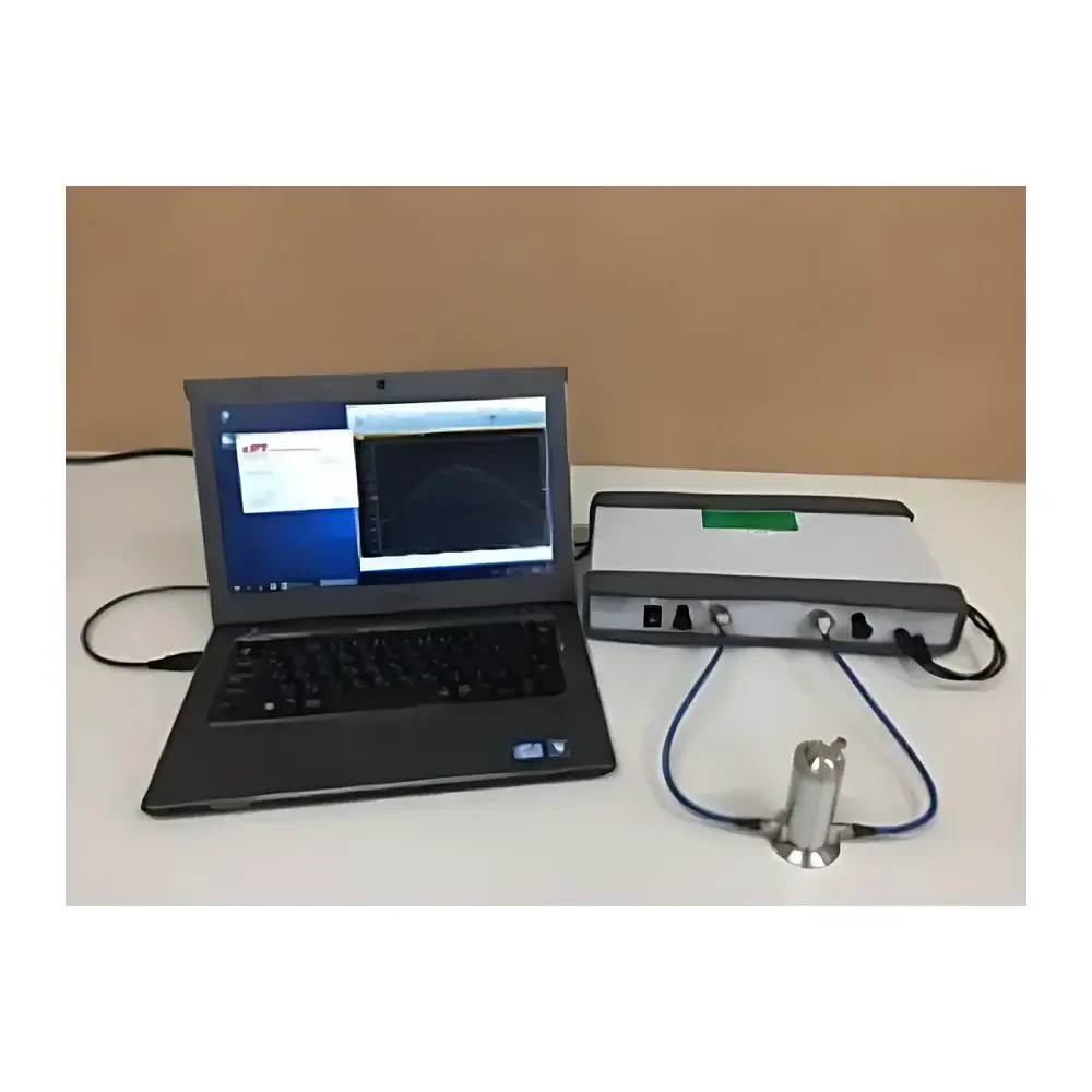
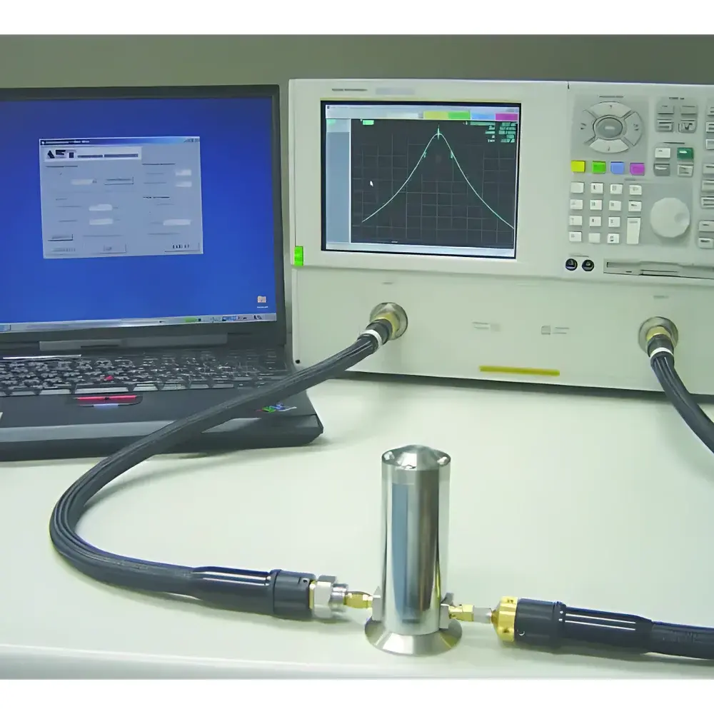
The AET Coaxial Resonant Cavity Dielectric Constant Analyzer is a precision instrument engineered for non-destructive, high-frequency electromagnetic characterization of solid and thin-film dielectric materials. It operates on the physical principle of resonant cavity perturbation theory: when a low-loss dielectric sample is introduced into a high-Q coaxial resonator, it induces measurable shifts in the cavity’s resonant frequency and quality factor (Q). These shifts are rigorously correlated to the real part (ε′) and imaginary part (ε″) of the complex permittivity via calibrated electromagnetic field models. Unlike broadband transmission-line or free-space methods, this cavity-based approach delivers superior signal-to-noise ratio and measurement reproducibility—especially critical for low-loss materials (tan δ < 0.01) used in millimeter-wave substrates and RF packaging. The system integrates CST Microwave Studio®-validated 3D electromagnetic simulations to compensate for field distortion at cavity-sample interfaces, ensuring traceable accuracy across the full 800 MHz to 9.4 GHz band.
Key Features
- Two interchangeable high-Q coaxial resonant cavities (Type A and Type B), each supporting five discrete, factory-calibrated resonant frequencies for targeted material evaluation.
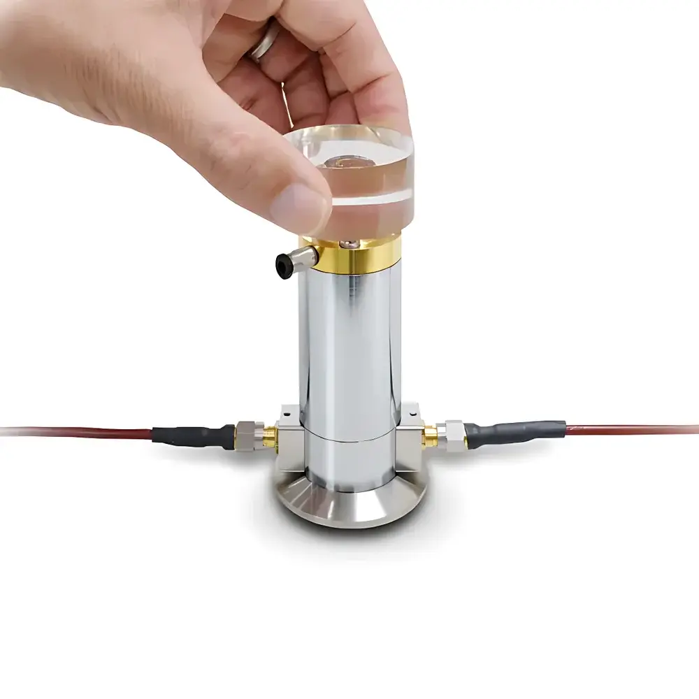
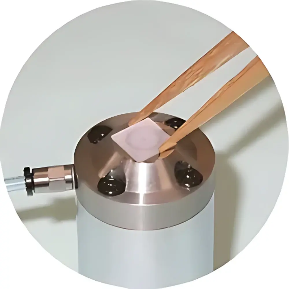
- No sample preparation required beyond a flat, contact-area surface—enabling rapid assessment of as-received wafers, laminates, ceramics, and flexible films without cutting, polishing, or metallization.
- Integrated feedback-controlled oscillator circuitry ensures stable excitation and precise lock-in detection of resonance parameters, minimizing drift and thermal sensitivity.
- Modular mechanical design accommodates samples up to 25 mm in diameter and 5 mm in thickness; compatible with standard probe station stages for in-situ or temperature-controlled measurements (when paired with optional environmental chambers).
- Compliance-ready architecture supports audit trails and user-access controls aligned with GLP and ISO/IEC 17025 laboratory management requirements.
Sample Compatibility & Compliance
The analyzer accepts a broad range of solid-state dielectrics—including printed circuit board laminates (e.g., FR-4, polyimide, PTFE-based CCL), low-k and high-k thin films (<1 µm to 100 µm), sintered ceramics (Al₂O₃, AlN, LTCC), semiconductor substrates (Si, SiC, GaN), and nanocomposite polymers. Its non-contact, plane-surface coupling eliminates edge effects common in parallel-plate or waveguide fixtures. All calibration procedures follow traceable standards referenced to NIST-traceable reference materials and are documented per ISO 17025 clause 6.5. Measurement uncertainty budgets—covering frequency stability, cavity Q-factor repeatability, and geometric tolerance contributions—are provided in the instrument validation report. The system meets electromagnetic compatibility (EMC) requirements per IEC 61326-1 and safety standards per IEC 61010-1.
Software & Data Management
The proprietary AET-Dielectric Suite provides guided workflow execution—from cavity selection and resonance search to permittivity extraction and uncertainty propagation. Raw S-parameter data (S₁₁ magnitude/phase) is logged in HDF5 format with embedded metadata (timestamp, operator ID, cavity serial number, ambient temperature/humidity). Export options include CSV, MATLAB .mat, and ASTM E2905-compliant XML for inter-laboratory data exchange. Audit logging records all parameter changes, calibration events, and report generations in accordance with FDA 21 CFR Part 11 requirements, including electronic signatures and immutable history tracking. Batch processing mode enables automated multi-sample analysis across heterogeneous material sets.
Applications
- Qualification of high-speed PCB substrates for 5G/mmWave applications (e.g., insertion loss modeling, impedance control verification).
- Development and process monitoring of low-loss filter dielectrics and ceramic antenna materials (e.g., BaTiO₃-based composites, MgTiO₃).
- Characterization of atomic-layer-deposited (ALD) and spin-coated thin films for gate dielectrics and passivation layers.
- Quality assurance of electronic packaging materials (EMI shielding composites, underfill epoxies, thermal interface materials).
- Research into emerging photonic and metamaterial structures where ε′ and tan δ govern dispersion and resonance behavior at sub-10 GHz bands.
FAQ
What sample geometries are supported?
Flat-bottomed solids with diameters between 10 mm and 25 mm and thicknesses from 0.1 mm to 5 mm. Flexible films require a rigid carrier substrate with ≥95% planarity over the contact area.
Is temperature-controlled measurement possible?
Yes—via integration with third-party cryogenic or heated sample stages (e.g., Linkam TS1500) using the system’s analog I/O interface and software-triggered acquisition synchronization.
How is calibration performed?
Using certified reference materials (CRMs) with known ε′ and tan δ values at specified frequencies; two-point calibration (air + reference) is executed prior to each measurement session.
Can the system measure anisotropic materials?
Not natively—measurement assumes isotropic dielectric response. For uniaxial or biaxial materials, orientation-dependent measurements require manual repositioning and post-processing correlation.
Does the system support custom frequency sweeps outside the five discrete resonances?
No—the cavity geometry fixes resonant modes; continuous sweeps are not supported. However, interpolation between adjacent cavity types (e.g., Type A → Type B) enables coverage across the full 0.8–9.4 GHz span.


