AET TE Cavity Resonator Dielectric Constant Tester
| Brand | AET |
|---|---|
| Origin | Japan |
| Manufacturer Type | Authorized Distributor |
| Product Origin | Imported |
| Model | TE Cavity Resonator |
| Price Range | USD 42,000 – 140,000 |
| Frequency Range | 10–40 GHz |
| Permittivity (εᵣ) | 1–5 |
| Accuracy | ±1% |
| Loss Tangent (tan δ) | 0.0001–0.01 |
| Accuracy | ±5% |
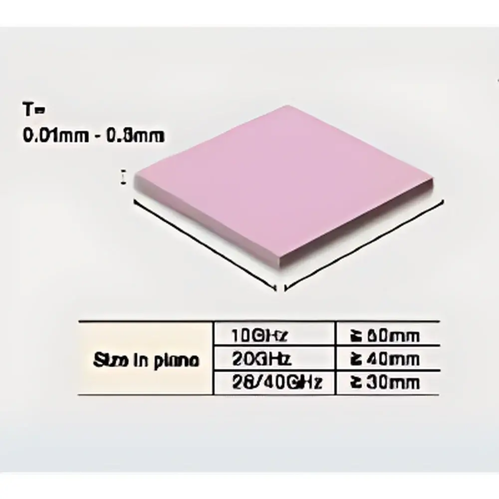
| Sample Thickness | 0.01–0.3 mm |
| Minimum Sample Size | 50×50 mm (at 10 GHz), 40×40 mm (at 20 GHz), 30×30 mm (at 28/40 GHz) |
| Compliance | JIS R1641, IPC-TM-650 2.5.5.13 |
| Measurement Geometry | In-plane (parallel to film surface) |
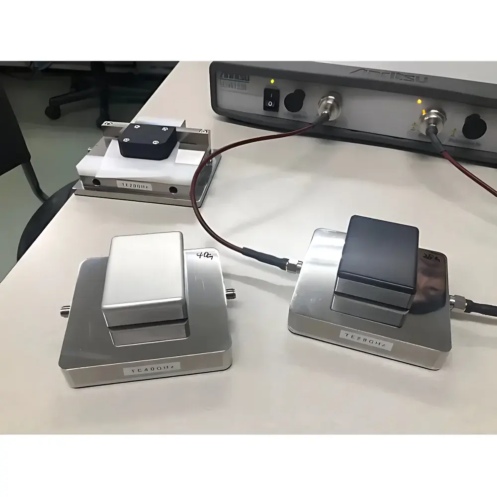
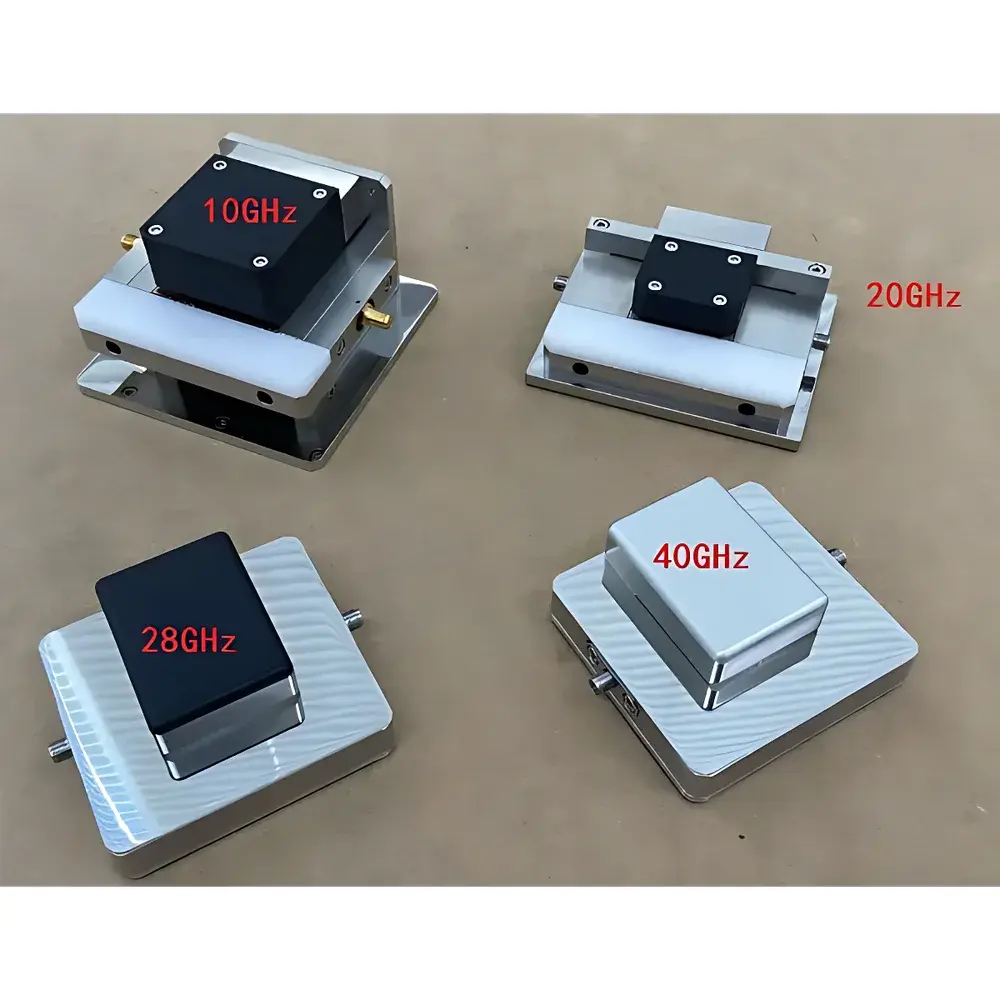
| Cavity Type | Split-cylinder TE-mode resonant cavity |
Overview
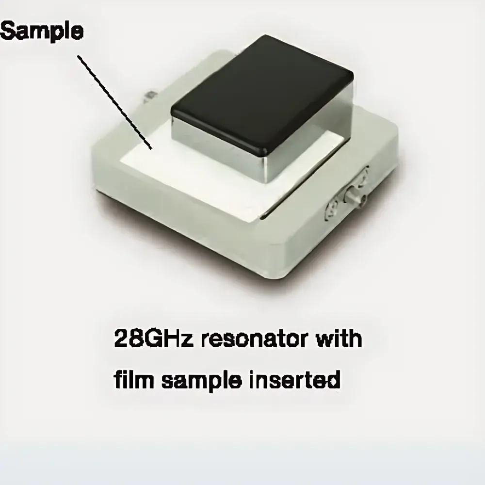
The AET TE Cavity Resonator Dielectric Constant Tester is a precision microwave metrology instrument engineered for non-destructive, high-resolution characterization of thin dielectric films in the 10–40 GHz frequency band. It operates on the principle of TE-mode (Transverse Electric) electromagnetic resonance within a split-cylinder metallic cavity, where the sample is inserted into a fixed, mechanically defined gap between two coaxially aligned cavity halves. This geometry ensures minimal perturbation of the fundamental TE011 or higher-order TE modes, enabling highly reproducible extraction of complex permittivity (ε* = ε’ − jε”) via resonance frequency shift (Δf) and quality factor (Q) degradation analysis. Designed specifically for sub-0.3 mm planar materials—including flexible polymers, brittle ceramics, low-loss laminates, and emerging 5G substrate candidates—the system delivers traceable, standards-aligned measurements critical for RF/microwave material qualification in advanced electronics manufacturing.
Key Features
- Split-cylinder TE-mode resonant cavity architecture with precision-machined, temperature-stable gap (±1 µm repeatability), eliminating clamping-induced stress and deformation errors common in conventional夹具-based methods;
- Frequency-agile operation across 10–40 GHz—covering key 5G NR bands (n257, n258, n260, n261) and millimeter-wave circuit design requirements;
- In-plane (parallel-to-surface) permittivity measurement orientation, directly relevant to signal propagation in PCB substrates, antenna dielectrics, and high-speed interconnect layers;
- High-loss-resolution capability: capable of resolving tan δ down to 1×10⁻⁴, essential for evaluating ultra-low-loss polyimides, liquid crystal polymers (LCP), and fluorinated ethylene propylene (FEP) films;
- Dedicated cavity modules per frequency point (e.g., 10 GHz, 20 GHz, 28 GHz, 40 GHz), each optimized for mode purity, field uniformity, and sensitivity to thin-film perturbation;
- No-contact sample positioning: samples rest freely within the gap without adhesive, pressure, or thermal loading—preserving integrity of soft, hygroscopic, or thermally sensitive films.
Sample Compatibility & Compliance
The system accommodates rigid, semi-rigid, and compliant thin-film specimens with thicknesses from 10 µm to 300 µm. Square-shaped samples are required to ensure uniform field interaction; minimum dimensions scale inversely with frequency to maintain >95% field confinement (≥50×50 mm at 10 GHz; ≥30×30 mm at 40 GHz). Compatible material classes include polymeric dielectrics (PI, LCP, PTFE composites), ceramic-polymer hybrids, spin-coated oxide films, semiconductor passivation layers, and metal-clad laminates (e.g., CCLs) when measured in unmetallized regions. All measurements comply with JIS R1641 (Methods for Determination of Dielectric Constant and Dissipation Factor of Advanced Ceramics) and IPC-TM-650 Test Method 2.5.5.13 (Dielectric Constant and Dissipation Factor by Split-Cylinder Resonator), supporting GLP/GMP documentation workflows and audit-ready data traceability.
Software & Data Management
Control and analysis are performed via AET’s proprietary CavityResonance™ software suite, which integrates real-time VNA (Vector Network Analyzer) data acquisition (compatible with Keysight PNA, Rohde & Schwarz ZNA, and Anritsu MS46500B platforms), automated resonance peak detection, and closed-form inversion algorithms based on rigorous cavity perturbation theory. The software generates full ε'(f), ε”(f), and tan δ(f) spectra, supports multi-point calibration using reference standards (e.g., fused silica, sapphire, air), and exports results in CSV, XML, and PDF formats compliant with ISO/IEC 17025 reporting requirements. Audit trails—including operator ID, timestamp, environmental conditions (optional humidity/temperature logging), and raw S-parameter files—are retained for FDA 21 CFR Part 11–compliant environments upon optional electronic signature module activation.
Applications
- Qualification of 5G mmWave substrate materials (e.g., low-Dk/Df laminates for base station antennas and phased-array modules);
- Development and process control of high-frequency printed circuit board (PCB) dielectrics, including FR-4 variants, hydrocarbon ceramics, and glass-reinforced PTFE;
- Characterization of thin-film encapsulants and passivation layers in advanced packaging (Fan-Out Wafer-Level Packaging, 2.5D/3D IC integration);
- R&D of low-loss dielectric filters, resonators, and metamaterial unit cells for satellite communications and radar systems;
- Material screening for flexible electronics, wearable sensors, and transparent conductive films where mechanical compliance precludes conventional probe-based methods;
- Supporting ASTM D2520, IEC 61282-11, and IEEE Std 1785.1–2021 test protocols for broadband dielectric spectroscopy of planar media.
FAQ
What is the physical measurement principle behind the TE cavity resonator?
It relies on perturbation of the resonant frequency and Q-factor of a TE-mode standing wave in a precisely dimensioned metallic cavity when a dielectric sample is introduced into a fixed gap—enabling calculation of ε’ and tan δ via first-order cavity perturbation theory.
Can the system measure metallized or patterned films?
Only uncoated dielectric regions can be measured; conductive layers must be fully removed or masked to avoid eddy-current distortion and field exclusion effects.
Is temperature-controlled measurement supported?
Yes—optional environmental chamber integration (−40°C to +150°C) with PID-controlled cavity mounting stage enables thermal coefficient of permittivity (TCP) and tan δ profiling.
How is calibration performed?
Using certified reference materials (e.g., NIST-traceable quartz, alumina, or air-gap null) and iterative error-model compensation for coupling port mismatch and cavity wall losses.
Does the system support batch testing of multiple samples?
Manual sample exchange is required per cavity module; however, automated sample loader integration is available as a factory-configured option for high-throughput QC labs.


")