Aisida XG6000 BGA Solder Joint Inspection System
| Brand | Aisida |
|---|---|
| Origin | Guangdong, China |
| Manufacturer Type | Authorized Distributor |
| Country of Origin | China |
| Model | XG6000 |
| Pricing | Upon Request |
Overview
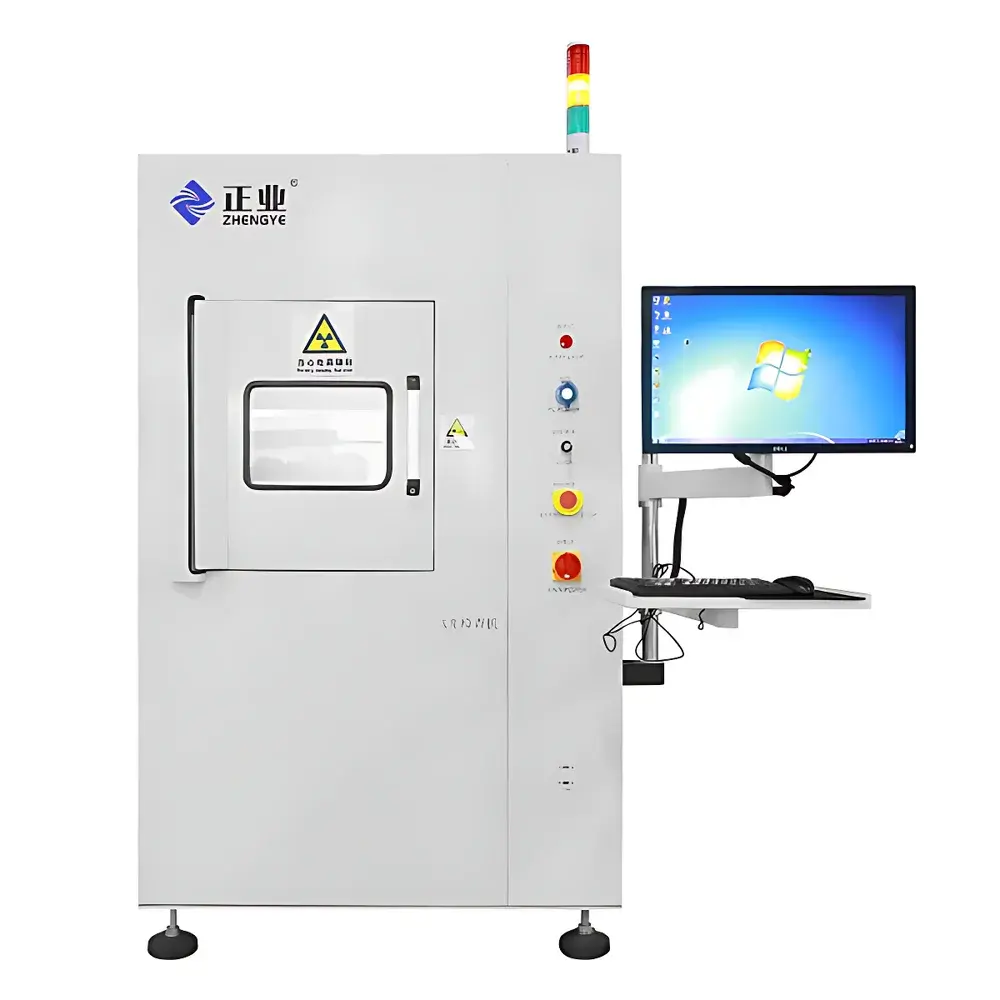
The Aisida XG6000 BGA Solder Joint Inspection System is a high-performance industrial X-ray inspection platform engineered for non-destructive evaluation of solder interconnects in advanced electronic assemblies. Based on transmission X-ray imaging principles, the system utilizes penetrating radiation to generate real-time, high-contrast cross-sectional views of internal structures without physical disassembly. It operates within the standard diagnostic energy range (typically 40–90 kV), optimized for resolving sub-100 µm features in lead-free and fine-pitch BGA, CSP, and QFN packages. Designed specifically for inline process validation and post-reflow quality assurance, the XG6000 supports traceable, repeatable defect identification in accordance with IPC-A-610 and J-STD-001 requirements for Class 2 and Class 3 electronics.
Key Features
- Sealed microfocus X-ray tube (≤5 µm focal spot) enabling high-resolution internal imaging of solder joints, voids, and intermetallic layers
- High-brightness, low-noise image intensifier coupled with digital CMOS detector for real-time dynamic imaging at up to 30 fps
- Motorized XYZ manipulator with precision tilt/rotation stages for multi-angle inspection and oblique view acquisition
- Integrated geometric magnification (up to 1000×) and digital zoom with pixel-level measurement calibration
- Ruggedized cabinet with interlocked shielding (≥1.0 mm Pb equivalent) compliant with IEC 61000-6-4 and local radiation safety regulations
- Onboard image processing engine supporting contrast enhancement, edge detection, and grayscale thresholding for automated void analysis
Sample Compatibility & Compliance
The XG6000 accommodates PCB substrates up to 400 × 300 mm and component heights up to 80 mm, supporting full-board BGA inspection including stacked-die and PoP configurations. It is validated for use with RoHS-compliant, lead-free SAC305 and SN100C solder alloys, as well as copper pillar and microbump interconnects. The system meets ISO 9001:2015 manufacturing controls and supports GLP/GMP-aligned documentation workflows. All image acquisition and measurement logs include embedded timestamps, operator ID, and instrument calibration status—enabling audit readiness per FDA 21 CFR Part 11 when paired with optional secure user authentication and electronic signature modules.
Software & Data Management
Equipped with proprietary Aisida VisionInspect™ v4.2 software, the XG6000 delivers standardized defect classification via configurable rule sets aligned with IPC-A-610 Rev. H criteria. Software features include automated void area quantification (per IPC-7095B Annex B), solder bridge detection using morphological segmentation, and statistical process control (SPC) charting for void percentage trends across production lots. Raw DICOM-compliant image data and annotated reports are exportable in PDF/A-1b, CSV, and XML formats. Audit trails record all parameter changes, measurement edits, and report generations with immutable timestamps—supporting regulatory review in medical device (ISO 13485) and automotive (IATF 16949) environments.
Applications
- Quantitative void analysis in BGA/CSP solder joints (size, distribution, and location relative to pad geometry)
- Detection of cold solder joints, insufficient wetting, solder bridging, and tombstoning in SMT reflow processes
- Internal structural verification of lithium-ion battery cells—including electrode alignment, separator integrity, and anode/cathode delamination
- Non-destructive evaluation of hermetic seals in MEMS packages and ceramic capacitors
- Inspection of wire bonding integrity, die attach voids, and leadframe defects in IC packaging
- Microstructural assessment of metal-ceramic interfaces in heating elements and power electronics modules
- Failure analysis root cause mapping for field returns involving latent solder fatigue or thermal cycling-induced cracks
FAQ
What is the minimum detectable void size under standard operating conditions?
Typical resolution allows reliable detection of spherical voids ≥25 µm in diameter at 5× geometric magnification; performance varies with material density and thickness.
Does the system support automated pass/fail reporting based on IPC criteria?
Yes—VisionInspect™ includes preloaded IPC-A-610 defect libraries and customizable acceptance thresholds for void area, bridging length, and solder fillet geometry.
Is radiation safety certification included with delivery?
Each unit ships with a factory-issued radiation leakage test report (per GBZ 138–2019 / IEC 62495) and installation guidance compliant with national regulatory authority requirements.
Can the XG6000 integrate with MES or factory automation systems?
Via TCP/IP and RESTful API, the system supports bidirectional data exchange with Siemens Opcenter, Rockwell FactoryTalk, and custom SCADA platforms for traceability and OEE monitoring.
What maintenance intervals are recommended for the X-ray tube and detector?
Scheduled preventive maintenance is advised every 1,500 operational hours; tube lifetime exceeds 8,000 hours under nominal 60 kV/0.5 mA operation with active cooling.
Related Products
")


")