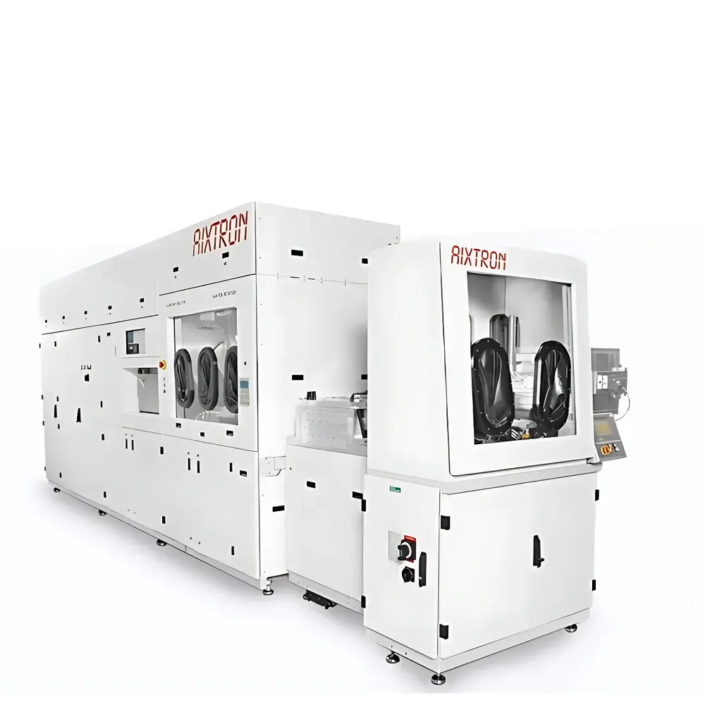
AIXTRON AIX 2800G4-TM Compound Semiconductor Deposition System
| Brand | AIXTRON |
|---|---|
| Origin | Germany |
| Model | AIX 2800G4-TM |
| Heating Method | Hot-Wall |
| Internal Chamber Dimensions | 15 × 4 in & 8 × 6 in |
| Reactor Configurations | 42 × 2 in / 11 × 4 in / 6 × 6 in |
| Wafer Throughput | High |
| Process Cycle Time | Rapid |
| Uniformity & Stability | Optimized for Production Yield |
Overview
The AIXTRON AIX 2800G4-TM Compound Semiconductor Deposition System is a production-proven, hot-wall metalorganic chemical vapor deposition (MOCVD) platform engineered for high-precision epitaxial growth of III–V and II–VI compound semiconductor layers. Designed and manufactured in Germany, this system leverages AIXTRON’s proprietary Close-Coupled Showerhead (CCS) technology and advanced thermal field control to deliver exceptional layer uniformity, compositional accuracy, and crystalline integrity across 2-inch to 6-inch wafers. It operates under ultra-high-purity process conditions—maintaining base pressures <1×10⁻⁶ mbar—and supports precise precursor delivery via mass flow controllers (MFCs), real-time pressure regulation, and closed-loop substrate temperature monitoring. The system is purpose-built for the scalable fabrication of optoelectronic and high-frequency devices, including GaN-based power HEMTs, GaAs/InP-based laser diodes and photodetectors, and AlGaInP-based LEDs.
Key Features
- Hot-wall reactor architecture with symmetric, low-thermal-gradient heating for superior radial temperature uniformity (±0.5 °C over 150 mm zone)
- Modular chamber design accommodating multiple reactor configurations: 42×2 in (for research-grade multi-wafer runs), 11×4 in (for 100–150 mm substrates), and 6×6 in (optimized for 150 mm GaN-on-Si or SiC wafers)
- Integrated in-situ optical monitoring (reflectance anisotropy spectroscopy and pyrometry) for real-time growth rate and surface morphology feedback
- Full automation via AIX G5 software suite with recipe-driven operation, event logging, and hardware interlock compliance per SEMI S2/S8 standards
- Dual-zone gas injection manifold enabling independent control of group-III and group-V precursors for stoichiometric tuning and interface engineering
- Robust safety architecture compliant with IEC 61508 SIL2 for hazardous gas handling (e.g., NH₃, TMGa, TMAI, PH₃)
Sample Compatibility & Compliance
The AIX 2800G4-TM supports heterogeneous epitaxy on technologically relevant substrates including sapphire (Al₂O₃), silicon (Si), silicon carbide (SiC), and bulk GaN. It accommodates wafer diameters from 2″ to 6″, with standard carrier configurations for both single-wafer and batch-mode processing. All process recipes are traceable and auditable in accordance with ISO 9001:2015 quality management requirements. The system meets key regulatory expectations for semiconductor manufacturing environments—including FDA 21 CFR Part 11 data integrity provisions when paired with validated electronic record modules—and supports GLP/GMP-aligned documentation workflows through optional audit trail extensions.
Software & Data Management
Control and monitoring are executed via AIXTRON’s G5 platform—a Windows-based, multi-user SCADA system featuring role-based access control, electronic signature support, and automated report generation (PDF/CSV). Process data—including MFC setpoints, chamber pressure, susceptor temperature, and in-situ optical signals—are timestamped at 100 Hz resolution and stored in a relational SQL database. Historical data export complies with ASTM E2500-17 guidelines for equipment qualification, and raw logs can be imported into third-party statistical process control (SPC) tools such as JMP or InfinityQS. Optional integration with MES systems (e.g., CIM300, FactoryTalk) enables real-time OEE tracking and preventive maintenance scheduling.
Applications
- GaN-based RF power amplifiers and millimeter-wave transistors for 5G infrastructure and satellite communications
- High-brightness blue/green micro-LED arrays for AR/VR displays and automotive lighting
- InP-based distributed feedback (DFB) lasers and electro-absorption modulators for coherent optical transceivers
- AlGaAs/GaAs quantum well infrared photodetectors (QWIPs) for thermal imaging and spectroscopy
- Buffer layer engineering for strain-compensated superlattices in high-electron-mobility transistor (HEMT) heterostructures
- Low-defect-density epitaxial templates for subsequent device fabrication steps (etching, metallization, passivation)
FAQ
What substrate sizes does the AIX 2800G4-TM support?
Standard configurations support 2″, 3″, 4″, and 6″ wafers; custom carriers enable 100 mm and 150 mm formats.
Is the system qualified for GaN-on-Si epitaxy?
Yes—the platform includes dedicated thermal ramp profiles, graded AlN/GaN buffer sequences, and in-situ stress compensation algorithms validated for 150 mm Si(111) substrates.
Can it be integrated into an existing cleanroom automation framework?
It supports SECS/GEM communication protocols and provides full SEMI E30/E37/E40 interface documentation for seamless factory automation integration.
What level of process repeatability is achievable?
Typical run-to-run thickness variation is ≤1.2% (3σ) for 200 nm GaN layers on 150 mm wafers, verified using ex-situ XRD and ellipsometry.
Does AIXTRON provide installation qualification (IQ) and operational qualification (OQ) documentation?
Yes—comprehensive IQ/OQ/ PQ protocols aligned with ASTM E2500-17 and ICH Q9 are included with each system shipment and supported by certified field engineers.


