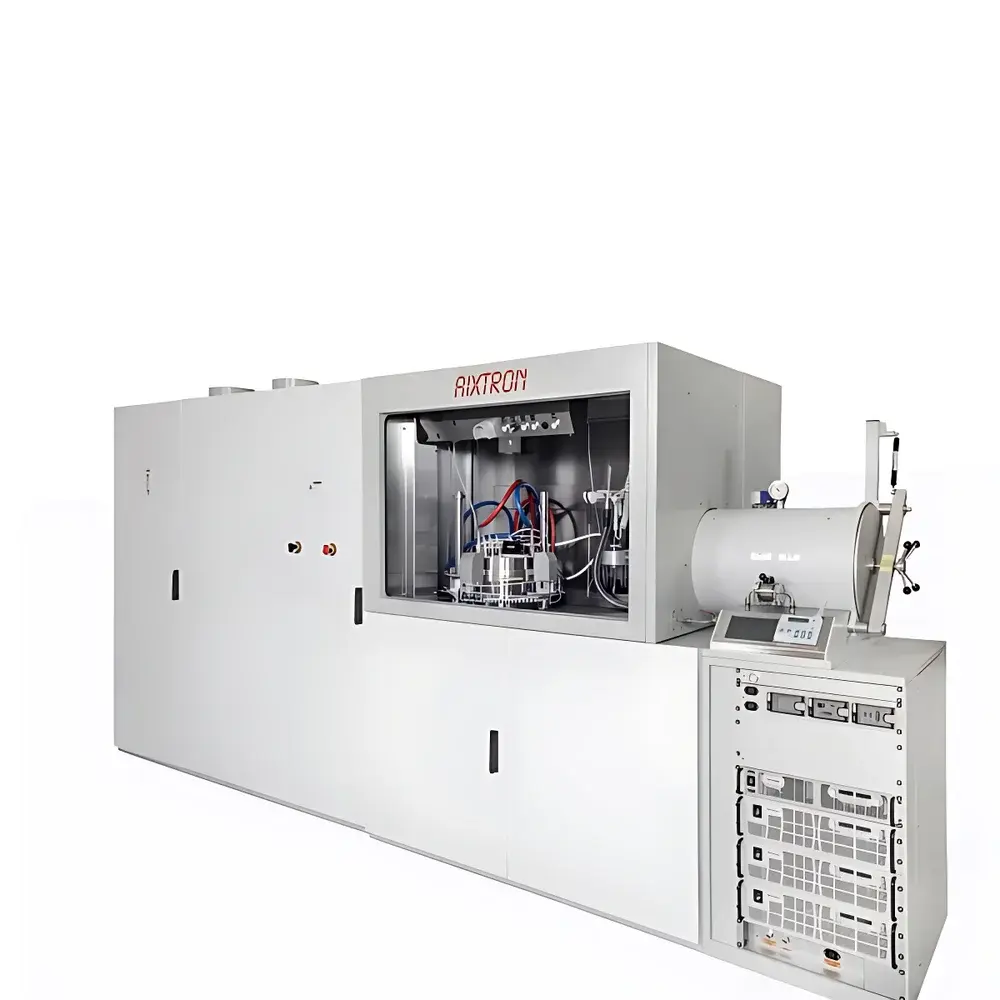
AIXTRON CCS Compound Semiconductor Deposition System
| Brand | AIXTRON |
|---|---|
| Origin | Germany |
| Equipment Type | Metalorganic Chemical Vapor Deposition (MOCVD) System |
| Reactor Architecture | Close-Coupled Showerhead® with Triple-Zone Heater |
| Maximum Substrate Temperature | 1400 °C |
| Substrate Configurations | 3×2″, 6×2″, 19×2″ wafers |
| In-situ Monitoring Options | LayTec EpiTT / EpiCurve®, AIXTRON Argus® Full-Wafer Temperature Mapping, AIXTRON Epison® Gas Concentration Sensor |
| Footprint | Compact Design for Lab and Pilot-Line Integration |
| Compliance | Designed for ISO Class 5–7 cleanroom environments |
| Software Platform | AIXTRON ProcessSuite™ with Audit Trail & Electronic Signature Support (21 CFR Part 11 compliant) |
Overview
The AIXTRON CCS (Compound Semiconductor Deposition) System is a high-precision metalorganic chemical vapor deposition (MOCVD) platform engineered for the epitaxial growth of compound semiconductor materials—including GaN, GaAs, InP, AlN, and related ternary and quaternary alloys. Operating on the fundamental principles of thermally activated surface reactions in low-pressure reactive gas environments, the CCS system enables atomic-layer control over film composition, thickness, doping profile, and crystallographic quality. Its core architecture integrates a Close-Coupled Showerhead® reactor—designed to ensure uniform precursor distribution across the substrate surface—and a triple-zone resistive heating system that delivers precise thermal gradients and exceptional radial temperature stability. This configuration supports reproducible growth kinetics across diverse material systems, from wide-bandgap nitrides used in high-power RF and optoelectronic devices to lattice-matched III–V heterostructures essential for high-efficiency photonic integrated circuits.
Key Features
- Close-Coupled Showerhead® Reactor: Optimized gas injection geometry minimizes boundary layer effects and enhances precursor utilization efficiency—critical for cost-sensitive MOCVD processes using expensive metalorganic precursors.
- Triple-Zone Heating System: Independent thermal control of susceptor center, edge, and dome zones enables fine-tuned compensation for heat loss and ensures ±0.5 °C radial uniformity at operating temperatures up to 1400 °C.
- Dynamic Gap Adjustment: Motorized vertical positioning of the showerhead allows real-time optimization of process gap (2–20 mm range), enabling rapid adaptation between high-throughput production and low-flow research conditions.
- Integrated Glovebox Interface (Optional): Enables air-sensitive precursor handling and substrate loading under inert atmosphere (O₂/H₂O < 1 ppm), supporting hydride-based chemistries (e.g., AsH₃, PH₃) without external transfer modules.
- Low-Flow Gas Architecture: Engineered for sub-100 sccm total carrier gas consumption during steady-state growth, reducing operational costs and improving safety in toxic precursor environments.
- Modular Vacuum & Exhaust Integration: Compatible with dry pumping systems and acid-scrubbed abatement units meeting SEMI S2/S8 safety guidelines and local environmental regulations.
Sample Compatibility & Compliance
The CCS system accommodates substrates ranging from 2-inch single-crystal wafers to clustered 19×2-inch configurations, supporting both conductive (SiC, Si) and insulating (sapphire, LiAlO₂) platforms. It is fully compatible with standard MOCVD-compatible wafer carriers (graphite or SiC-coated susceptors) and supports in-situ etch-and-grow sequences via programmable H₂/NH₃ ramping protocols. All hardware and software components conform to IEC 61000-6-2/6-4 electromagnetic compatibility standards and meet CE Machinery Directive 2006/42/EC requirements. The system’s process control firmware implements full audit trail logging, electronic signatures, and role-based access—fully aligned with FDA 21 CFR Part 11 and EU Annex 11 expectations for GMP-compliant semiconductor pilot-line operations.
Software & Data Management
Controlled by AIXTRON ProcessSuite™ v5.x, the CCS platform provides deterministic recipe execution with sub-second timing resolution, synchronized data acquisition from up to 16 analog/digital I/O channels, and real-time feedback loops for temperature, pressure, and gas flow regulation. Process logs—including chamber wall temperature profiles, mass flow controller setpoints, and in-situ optical signals—are stored in encrypted SQLite databases with SHA-256 hashing for integrity verification. Export formats include CSV, HDF5, and SECS/GEM-compliant HSMS streams for integration into MES/SPC infrastructure. Remote diagnostics and predictive maintenance alerts are accessible via secure TLS 1.3 web interface with optional OPC UA server integration.
Applications
The CCS system serves as a foundational tool in R&D and pilot manufacturing of advanced compound semiconductor devices. Key application domains include: GaN-on-Si power transistors for automotive traction inverters; InGaN-based micro-LED arrays for AR/VR displays; AlGaAs/GaAs quantum well lasers for fiber-optic communications; InP-based heterojunction bipolar transistors (HBTs) for 5G mmWave front-end modules; and AlN-based SAW/BAW filters for RF signal conditioning. Its ability to maintain stoichiometric fidelity across multi-layer superlattices (e.g., AlGaN/GaN HEMT stacks) and graded buffer layers has been validated in peer-reviewed studies published in Journal of Crystal Growth and IEEE Transactions on Electron Devices.
FAQ
What substrate sizes does the CCS system support?
Standard configurations include 3×2″, 6×2″, and 19×2″ clusters; custom susceptor designs for non-standard geometries (e.g., 100 mm hexagonal SiC wafers) are available upon request.
Is the system qualified for hydride-based chemistry (e.g., AsH₃, PH₃)?
Yes—when equipped with the integrated glovebox option and certified abatement interface, the CCS meets SEMI E77 and OSHA PEL requirements for Class B hydride handling.
Can the system be upgraded for production-scale throughput?
All CCS platforms use the same reactor core and control architecture as AIXTRON’s production-grade AIX 2800G4 systems, enabling seamless transition from lab-scale development to volume manufacturing via hardware retrofit and software license expansion.
What level of in-situ monitoring integration is supported?
LayTec EpiTT reflectance interferometry, EpiCurve® curvature mapping, AIXTRON Argus® full-wafer pyrometry, and Epison® gas-phase FTIR sensing can be simultaneously commissioned with synchronized timestamp alignment to process events.
Does the system comply with FDA 21 CFR Part 11 for regulated environments?
Yes—ProcessSuite™ includes configurable audit trails, electronic signatures, user authentication (LDAP/Active Directory), and data integrity safeguards required for GLP/GMP audits in compound semiconductor device qualification workflows.


