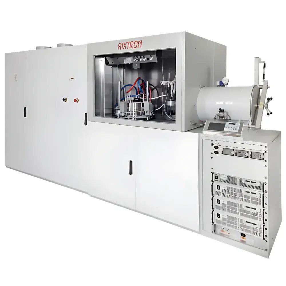
AIXTRON Customized MOCVD System for Semiconductor Thin-Film Epitaxy
| Brand | AIXTRON |
|---|---|
| Origin | Germany |
| Model | Customized |
| Heating Method | Tungsten Filament with Triple-Zone Temperature Control (up to 1400 °C) |
| Substrate Compatibility | 3×2 inch, 1×4 inch, 1×3 inch, 1×2 inch |
| Ga₂O₃ Growth Rate | >3 µm/h |
| Ga₂O₃ Surface Roughness (5 µm × 5 µm, AFM on Ga₂O₃ substrate) | ≤1.0 nm |
| Reaction Chamber | Adjustable showerhead-to-substrate spacing (5–25 mm) |
| In-situ Monitoring | Real-time wafer surface temperature mapping and warp measurement |
| Application Scope | Ga₂O₃, GaN, InP, GaAs, InSb, GaInNAs, II–VI compound semiconductors |
| Compliance | Designed for ISO Class 5 cleanroom integration and compatible with semiconductor fab infrastructure (SEMI S2/S8, SEMI E10) |
Overview
The AIXTRON Customized Metalorganic Chemical Vapor Deposition (MOCVD) System is an engineered platform for high-precision epitaxial growth of compound semiconductor thin films in research, development, and pilot-scale manufacturing environments. Operating on the fundamental principle of thermal decomposition of metalorganic precursors—delivered via inert carrier gases into a heated reaction chamber—the system enables controlled, layer-by-layer crystalline growth on semiconductor substrates. Its core architecture integrates thermally stable tungsten filament heating with triple-zone temperature regulation, supporting maximum process temperatures up to 1400 °C. This capability is essential for the synthesis of wide-bandgap materials such as β-Ga₂O₃ and high-performance III–V compounds including GaN, InP, and GaAs. The reactor features a dynamically adjustable showerhead-to-substrate gap (5–25 mm), allowing precise tuning of precursor residence time and gas-phase uniformity across the wafer surface—a critical parameter influencing film stoichiometry, thickness uniformity, and defect density.
Key Features
- Tungsten-filament-based heating system with independent triple-zone thermal control for exceptional radial and axial temperature homogeneity.
- Configurable substrate handling accommodating multiple formats: standard configurations include 3×2 inch, 1×4 inch, 1×3 inch, and 1×2 inch wafers; carrier-exchange mode supports extended layouts such as 6×2 inch, 3×3 inch, or 1×6 inch for flexible throughput scaling.
- In-situ real-time monitoring suite comprising pyrometric wafer surface temperature mapping and optical interferometric wafer warp detection—enabling closed-loop process stabilization during high-temperature epitaxy.
- Ga₂O₃-specific optimization: demonstrated growth rates exceeding 3 µm/h with surface roughness ≤1.0 nm (measured by atomic force microscopy over 5 µm × 5 µm areas on native Ga₂O₃ substrates).
- Modular vacuum and gas delivery architecture compliant with ultra-high-purity (UHP) gas standards (ISO 8573-1 Class 1 for particles, Class 2 for moisture/oil), minimizing contamination risk in sensitive heteroepitaxial processes.
Sample Compatibility & Compliance
This MOCVD platform supports epitaxial growth on technologically relevant substrates including sapphire, SiC, Si, and native Ga₂O₃, with proven compatibility for both polar and semi-polar orientations. It meets structural and operational requirements for integration into Class 5 (ISO 14644-1) cleanroom facilities. All hardware interfaces and safety interlocks conform to SEMI S2 (Health and Safety Guidelines) and SEMI S8 (Environmental, Health, and Safety Guideline for Semiconductor Manufacturing Equipment) standards. Gas cabinet integration follows NFPA 55 and local hazardous material regulations. While not pre-certified for GMP production, the system’s design permits validation under ICH Q5D, USP , and ISO/IEC 17025 frameworks when deployed within qualified laboratory or pilot-line settings.
Software & Data Management
The system operates under AIXTRON’s proprietary Process Control Software (PCS), providing full recipe management, real-time parameter logging (temperature profiles, gas flow rates, pressure transients, and in-situ sensor outputs), and event-driven alarm handling. Data export adheres to ASTM E1578-19 (Standard Guide for Laboratory Information Management Systems) conventions and supports CSV, HDF5, and XML formats. Audit trail functionality satisfies FDA 21 CFR Part 11 requirements for electronic records and signatures when configured with user authentication, role-based access control, and immutable log archiving. Integration with enterprise MES systems (e.g., Siemens Opcenter, Applied Materials EnVision) is supported via OPC UA and SECS/GEM protocols.
Applications
- Development of high-breakdown-voltage power electronics using β-Ga₂O₃ and AlGaN/GaN heterostructures.
- Epitaxial growth of infrared photodetectors and laser diodes based on InSb and InP platforms.
- Research on dilute nitride alloys (e.g., GaInNAs) for telecom-band optoelectronics and quantum well solar cells.
- Deposition of II–VI compound layers (e.g., ZnSe, CdTe) for radiation-hardened sensors and thin-film photovoltaics.
- Process transfer from R&D to pilot-line scale, leveraging identical thermal and gas-dynamic boundary conditions across configurations.
FAQ
What substrate sizes does this MOCVD system support natively?
Standard configurations support 3×2 inch, 1×4 inch, 1×3 inch, and 1×2 inch substrates. Carrier-exchange operation extends flexibility to non-standard arrangements including 6×2 inch, 3×3 inch, and 1×6 inch layouts.
Is real-time temperature mapping available across the entire wafer surface?
Yes—the integrated multi-point pyrometry system generates spatially resolved temperature maps at sub-second temporal resolution, enabling dynamic correction of thermal gradients during growth.
Can the system be validated for GLP or GMP-compliant environments?
While delivered as a research-grade tool, its software architecture, audit trail implementation, and hardware traceability pathways are fully extensible to GLP (OECD Principles) and GMP (ICH Q7) validation protocols when commissioned with appropriate documentation packages and IQ/OQ/PQ execution support.
What is the typical maintenance interval for the tungsten heating elements?
Under standard operating conditions (≤1300 °C, N₂/H₂ ambient), tungsten filaments exhibit service lifetimes exceeding 1,500 hours. AIXTRON provides predictive maintenance scheduling tools based on cumulative thermal stress metrics logged in the PCS database.


