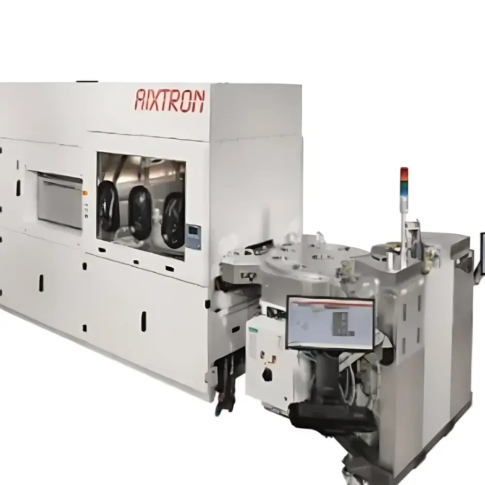
AIXTRON G10-SiC Chemical Vapor Deposition System
| Brand | AIXTRON |
|---|---|
| Origin | Germany |
| Model | G10-SiC |
| Wafer Compatibility | 150 mm & 200 mm |
| Application Focus | SiC Epitaxy for Power Devices |
Overview
The AIXTRON G10-SiC is a high-performance, industrial-grade chemical vapor deposition (CVD) system engineered specifically for the epitaxial growth of silicon carbide (SiC) layers on conductive and semi-insulating 150 mm and 200 mm silicon carbide substrates. Utilizing advanced hot-wall or cold-wall CVD architecture—depending on configuration—the system enables precise control over gas-phase precursor chemistry (e.g., silane, propane, and dopant sources such as nitrogen or aluminum halides), substrate temperature (up to 1700 °C), pressure (sub-atmospheric to near-atmospheric), and gas flow dynamics. This level of process control is essential for producing high-quality, low-defect-density SiC epilayers used in vertical power devices including trench-gate MOSFETs, JBS diodes, and high-voltage Schottky barrier diodes. The G10-SiC platform is designed to meet the stringent requirements of SiC device manufacturing, where layer thickness uniformity (<±1.5% across 200 mm wafers), doping concentration reproducibility (±3% relative), and crystallographic quality (low micropipe and basal plane dislocation density) directly impact breakdown voltage, on-resistance, and long-term reliability.
Key Features
- Modular 4-reactor cluster configuration enabling parallel process development, qualification, and high-volume pilot production—maximizing tool utilization and reducing time-to-data.
- Dual-wafer-size capability (150 mm and 200 mm) with interchangeable susceptor assemblies and optimized thermal field design to ensure uniform radial temperature distribution across both formats.
- Integrated real-time in-situ monitoring options—including optical pyrometry, laser interferometry, and residual gas analysis (RGA)—to support closed-loop process control and endpoint detection.
- High-temperature graphite susceptor and heater assembly rated for continuous operation up to 1700 °C, with rapid thermal ramping (≥100 °C/min) and sub-0.5 °C stability under steady-state conditions.
- Gas delivery system compliant with SEMI S2/S8 safety standards, featuring mass flow controllers (MFCs) with <1% full-scale accuracy and redundant purge pathways for hazardous precursors (e.g., NH₃, AlCl₃).
- Full integration with AIXTRON’s proprietary Process Control Software (PCS), supporting recipe-based execution, parameter logging, and audit-trail generation aligned with FDA 21 CFR Part 11 and ISO 9001 requirements.
Sample Compatibility & Compliance
The G10-SiC accommodates standard 150 mm and 200 mm SiC wafers—both n-type (N-doped) and p-type (Al-doped)—as well as engineered substrates such as off-axis 4H-SiC (4° toward [11–20]) and 6H-SiC. Substrate holders are compatible with standard wafer carriers (FOUPs/SMIF pods) and support backside helium cooling for improved thermal management during high-power growth. The system meets CE marking requirements and conforms to IEC 61000-6-2 (EMC immunity) and IEC 61000-6-4 (EMC emission) standards. All hardware and software components are validated per ISO/IEC 17025 guidelines for materials characterization laboratories, and the platform has been deployed in multiple Fraunhofer Institute cleanroom facilities operating under GLP-compliant workflows.
Software & Data Management
AIXTRON’s PCS provides a secure, role-based user interface with multi-level access control (operator, engineer, administrator). Process data—including temperature profiles, MFC setpoints, chamber pressure logs, and in-situ sensor outputs—are timestamped and stored in an encrypted SQLite database with automatic daily backup to network-attached storage (NAS). Raw datasets export in CSV and HDF5 formats for post-processing in MATLAB, Python (NumPy/Pandas), or industry-standard metrology platforms (e.g., KLA Candela, Bruker Dektak). Audit trails record all user actions, parameter changes, and system events with immutable timestamps—fully traceable for internal quality audits or external regulatory reviews (e.g., IATF 16949 for automotive-grade SiC qualification).
Applications
- Development and scaling of 600 V–1700 V SiC power devices, including planar and trench-gate MOSFETs, JFETs, and PIN diodes for EV traction inverters and onboard chargers.
- Growth of thick (>100 µm) drift layers for high-breakdown-voltage Schottky diodes used in photovoltaic string inverters and wind turbine converters.
- Research into polytype control (4H vs. 6H), defect engineering (VSi, CSi antisites), and heteroepitaxy on silicon substrates for cost-sensitive applications.
- Process qualification for AEC-Q101-compliant SiC discrete devices and AQG-324-qualified modules intended for rail and aerospace power systems.
- Support for DOE-funded initiatives targeting >99.999% wafer yield in 200 mm SiC epitaxy lines through statistical process control (SPC) integration.
FAQ
What substrate orientations and polytypes does the G10-SiC support?
The system is optimized for off-axis (4°) 4H-SiC wafers but supports growth on 6H-SiC, 3C-SiC on Si, and semi-insulating substrates via adjustable susceptor geometry and tailored precursor injection sequencing.
Is remote diagnostics and predictive maintenance available?
Yes—via optional AIXTRON Remote Service Module (RSM), which enables secure TLS-encrypted connection for real-time health monitoring, fault code analysis, and scheduled calibration alerts based on cumulative thermal cycles and gas exposure metrics.
Can the system be upgraded for 300 mm wafer processing?
While the current G10-SiC platform is certified for 200 mm, AIXTRON offers a technology roadmap extension path—including mechanical redesign, thermal modeling updates, and new susceptor tooling—for future 300 mm SiC epitaxy, subject to joint feasibility assessment with Fraunhofer IISB.
How is process repeatability validated across multiple reactors?
Each reactor undergoes independent thermal mapping and gas-flow profiling prior to commissioning; cross-reactor matching is verified using reference wafers with standardized test structures and certified metrology (SIMS, XRD, LBIC) at Fraunhofer’s accredited labs.
Does the system comply with semiconductor fab environmental standards?
Yes—the G10-SiC meets Class 100 (ISO 5) cleanroom compatibility requirements, includes integrated HEPA filtration for purge gases, and features fully sealed RF-shielded electronics enclosures meeting SEMI F47 voltage sag immunity specifications.


