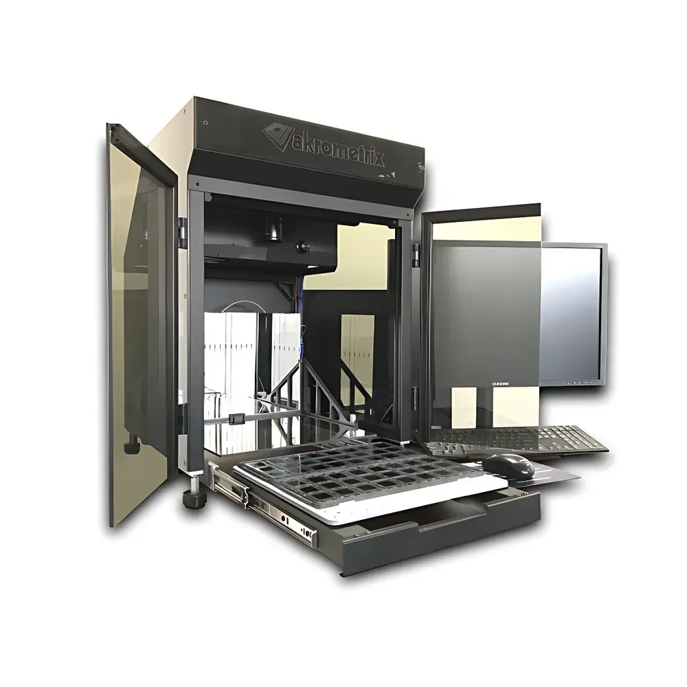
Akrometrix TTSM Tabletop Shadow Moiré Warpage Metrology System
| Brand | Akrometrix |
|---|---|
| Origin | USA |
| Model | TTSM |
| Measurement Principle | Non-contact shadow moiré interferometry |
| Temperature Range | Ambient to 300 °C (optional -50 °C to 300 °C) |
| Z-axis Resolution | ≤1.25 µm (AKM600P variant) |
| Field of View | Up to 600 mm × 600 mm (AKM600P), 48 mm × 64 mm (DFP), 70 mm circular (CRE) |
| Data Acquisition Speed | <2 s per full-field measurement (up to 1.4 million data points) |
| Compliance | JEDEC JESD22-B112, JEITA ED-7306, IPC TM-650 2.4.22 (Bow & Twist), IPC-9641, ASTM E2923 |
Overview
The Akrometrix TTSM Tabletop Shadow Moiré Warpage Metrology System is a precision optical metrology platform engineered for non-contact, full-field, high-resolution measurement of thermal deformation and out-of-plane warpage in microelectronic packages, substrates, PCBs, and advanced packaging structures—including fan-out wafer-level packages (FOWLP), QFNs, BGAs, and heterogeneous integration assemblies. Based on shadow moiré interferometry—a geometric optical technique—the TTSM projects a Ronchi grating pattern onto the sample surface and captures its shadow with a perpendicular camera. Interference between the reference grating and its projected shadow generates a moiré fringe pattern; phase-stepping algorithms decode local fringe displacement to reconstruct sub-micron vertical topography across the entire field of view. Unlike point-scanning or profilometric methods, the TTSM delivers instantaneous, distortion-free, single-shot 3D surface maps—enabling quantitative analysis of coplanarity, signed warpage, bow, twist, and localized deformation kinetics during thermal transients.
Key Features
- Full-field, non-contact measurement with no mechanical probing or surface contact—preserving solder integrity and enabling post-reflow co-planarity assessment of live solder balls.
- Sub-second acquisition (<2 s) of up to 1.4 million 3D data points per frame, supporting real-time thermal deformation tracking from ambient to 300 °C.
- Modular thermal control architecture: infrared heating + forced convection cooling for precise ramp rates (up to 1.5 °C/s) and uniform temperature distribution—validated per JEDEC JESD22-B112 thermal profile specifications.
- Multi-configurable optical modules: Standard TTSM, DFP (Digital Fringe Projection) for stepped/intermittent surfaces, CRE (Convection Reflow Emulation) for production-representative airflow-based thermal cycling, and AKM600P for 600 mm × 600 mm wafer-scale FOV.
- Z-axis resolution down to 1.25 µm (AKM600P) and 5 µm (DFP), traceable to NIST standards via factory calibration protocols compliant with ISO/IEC 17025 requirements.
- Integrated strain and CTE calculation engine using in-plane displacement fields derived from optional DIC 2.0 add-on module (in-plane resolution <1.0 µm; strain resolution <150 µε).
Sample Compatibility & Compliance
The TTSM accommodates samples ranging from 0.5 mm × 0.5 mm (with DFP option) to 600 mm × 600 mm (AKM600P), including bare die, molded packages, panelized PCBs, ceramic substrates, and FOWLP redistribution layers. It supports measurement of both continuous and discontinuous topographies—such as solder ball arrays with height variations, stepped package lids, and embedded passive structures—without requiring reflective coatings or fiducial markers. All measurement outputs conform to industry-standard warpage metrics: JEDEC JESD22-B112 (full-field signed warpage), JEITA ED-7306 (normalized diagonal warpage), IPC TM-650 Method 2.4.22 (bow and twist), IPC-9641 (BGA-to-PCB gap analysis), and CTE-derived mean strain profiles. System validation documentation includes traceable uncertainty budgets aligned with ISO/IEC 17025 and supports GLP/GMP audit readiness.
Software & Data Management
Akrometrix Studio 8.2 is a modular, Windows-based software suite delivering end-to-end workflow automation—from experimental setup and thermal profiling to quantitative warpage analytics and statistical process control (SPC). The platform features real-time pass/fail decision logic based on user-defined criteria (e.g., max allowable warpage per IPC-9641 thresholds), automated sample tracking for unattended multi-sample runs, and synchronized thermal event logging. Analysis modules include 3D surface rendering, cross-sectional slice extraction, HNP/HOP (head-in-pillow) defect mapping, short/open circuit gap visualization, and statistical reporting (Cp/Cpk, X-bar R charts). Raw data is stored in vendor-neutral HDF5 format with embedded metadata (temperature, time stamp, instrument ID, calibration ID), ensuring compliance with FDA 21 CFR Part 11 requirements for electronic records and signatures when configured with audit trail and user access controls.
Applications
The TTSM serves critical roles across the microelectronics value chain: in R&D for package substrate material selection and mold compound optimization; in process development for reflow profile tuning and underfill cure characterization; in manufacturing for first-article inspection and line-side SPC monitoring; and in reliability engineering for thermal cycling qualification (e.g., -50 °C to 300 °C) and failure root cause analysis. Specific use cases include BGA coplanarity verification pre- and post-reflow, warpage-induced tombstoning prediction, FOWLP wafer-level stress mapping, CTE mismatch quantification between die/substrate/encapsulant, and interposer warpage compensation in 2.5D/3D heterogeneous integration stacks. Its compatibility with JEDEC-standard test vehicles enables direct correlation with assembly yield loss models.
FAQ
What thermal profiles can the TTSM replicate?
The system supports programmable heating/cooling ramps from ambient to 300 °C (standard) or -50 °C to 300 °C (optional low-temp chamber), with convection-based CRE modules emulating industrial reflow ovens per J-STD-020 and JEDEC JESD22-B112 specifications.
Does the TTSM require sample coating or preparation?
No—shadow moiré is inherently compatible with bare metal, solder, laminate, and molded surfaces; no spray, tape, or fiducials are needed.
Can it measure warpage during actual reflow?
Yes—real-time acquisition at <2 s/frame enables capture of dynamic warpage evolution throughout the entire thermal cycle, synchronized with thermocouple or IR pyrometer inputs.
Is NIST-traceable calibration available?
Yes—each system ships with a certificate of calibration traceable to NIST Standard Reference Materials (SRMs), including step-height artifacts and thermal uniformity validation reports.
How does TTSM compare to laser scanning or white-light interferometry?
Unlike scanning techniques, TTSM provides true full-field data without stitching artifacts or motion-induced error; unlike interferometry, it is insensitive to surface reflectivity, coherence noise, or vibration—making it robust in production environments.


