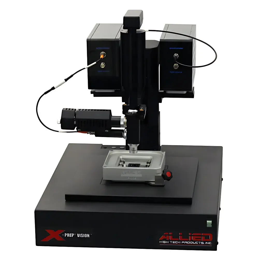
Allied X-PREP® VISION™ Substrate Thickness Metrology System
| Brand | Allied |
|---|---|
| Origin | USA |
| Model | X-PREP® VISION™ |
| Measurement Principle | Infrared Reflectance Interferometry (with optional visible-light spectrometry) |
| Thickness Range | 10 µm – 1 mm (standard) |
| Stage Travel | 100 mm × 100 mm (X/Y) |
| Auto-Focus Z-Axis | Motorized, <1 s acquisition time per point |
| Measurement Modes | Single-point or multipoint grid scan |
| Edge & Corner Detection | Automatic, with theta correction and X/Y-defined edge exclusion |
| Software Platform | Allied X-Correct™ (proprietary), .NET extensible |
| Data Export | Native Windows-compatible formats (CSV, BMP, TIFF, XML) |
| Camera Requirement | CCD camera (#15-50020) required unless #15-51000 Spectrometer is installed |
| Surface Roughness Tolerance | ≤15 µm Ra |
| Physical Dimensions | 355 mm (W) × 431 mm (D) × 483 mm (H) |
| Warranty | 12 months limited |
Overview
The Allied X-PREP® VISION™ is a non-contact, motorized substrate thickness metrology system engineered for precision measurement of semiconductor wafers, compound semiconductor substrates, optical crystals, and thin-film-coated materials. It operates on the principle of infrared reflectance interferometry: a collimated IR beam is directed onto the sample surface, where interference patterns generated by reflections from the top surface and substrate–back interface are captured and resolved in the frequency domain. The resulting phase shift and fringe periodicity are directly correlated to optical path difference, enabling sub-micron thickness resolution without physical contact or destructive sampling. When configured with the optional #15-51000 Visible Light Spectrometer accessory, the system extends its capability into the nanoscale regime (down to 15 nm), supporting applications such as ultra-thin SOI layer characterization, epitaxial film monitoring, and post-CMP thickness verification.
Key Features
- Multipoint automated grid scanning with programmable coordinate mapping—enabling full-wafer uniformity analysis across 100 mm × 100 mm travel range
- Motorized XYZ stage with real-time auto-focus (<1 s acquisition per measurement point) and integrated theta-axis correction for angular misalignment compensation
- Intelligent edge and corner detection algorithm that dynamically aligns the measurement grid with the X-PREP® fixture geometry—ensuring repeatable positional registration between preparation and metrology workflows
- Configurable edge exclusion zone via user-defined X/Y offsets, minimizing edge-effect artifacts in thickness profiles
- “Drive to Coordinate” software navigation for rapid repositioning to any stored measurement location—critical for failure analysis and cross-platform correlation
- Simultaneous visualization of results in 2D heatmaps or 3D topographic plots, with overlay support for reference CAD outlines and mask layer data
- Fully integrated X-Correct™ software suite featuring scripting support via .NET API—enabling custom automation sequences, SPC integration, and batch report generation
- Native compatibility with standard Windows data export protocols (CSV, TIFF, XML), facilitating seamless import into statistical process control (SPC) platforms and LIMS environments
Sample Compatibility & Compliance
The X-PREP® VISION™ supports a broad library of over 130 pre-calibrated materials—including GaAs, InP, SiC, Al2O3 (sapphire), SiGe, GaN, photoresists, and fused silica—each with empirically validated refractive index dispersion models across the operational IR spectrum (1.0–1.7 µm). The system accommodates rigid planar substrates up to 150 mm in diameter and thicknesses up to 1 mm. Its non-destructive methodology complies with ASTM F390-22 (Standard Test Method for Measuring Thickness of Transparent Films Using Interferometry) and aligns with ISO/IEC 17025 requirements for measurement traceability when used with NIST-traceable calibration standards. For regulated environments, X-Correct™ supports audit-ready logging, user-access controls, and electronic signature functionality consistent with FDA 21 CFR Part 11 and GLP/GMP documentation standards.
Software & Data Management
X-Correct™ is a Windows-based metrology platform developed exclusively for Allied’s X-PREP® ecosystem. It provides real-time signal processing, spectral deconvolution, and multi-layer thickness inversion algorithms optimized for single- and dual-interface systems. All measurement sessions generate timestamped, metadata-rich project files containing raw interferograms, calibration history, operator ID, environmental conditions (optional sensor input), and full audit trails. The software architecture supports scheduled calibration reminders, instrument health diagnostics, and remote firmware updates. Data export adheres to ASTM E1392-21 (Standard Practice for Electronic Transfer of Laboratory Data) and integrates natively with enterprise MES and QMS platforms via OPC UA or RESTful API extensions.
Applications
- Thickness verification of polished wafers prior to epitaxial growth or device fabrication
- Post-grinding/post-lapping thickness uniformity assessment for compound semiconductor substrates
- Quantitative evaluation of thin-film removal rates during CMP process development
- SOI layer thickness mapping for FD-SOI technology nodes
- Quality control of optical window substrates (e.g., MgF2, CaF2) requiring ±0.1% thickness tolerance
- Failure analysis support—correlating localized thickness variation with electrical test anomalies
- Process validation for wafer-level packaging and through-silicon via (TSV) thinning operations
FAQ
Is the CCD camera included with the base system?
No—the #15-50020 CCD camera is an optional accessory and must be purchased separately unless the #15-51000 Visible Light Spectrometer is ordered, which includes integrated imaging capability.
Can the system measure transparent films on opaque substrates?
Yes, provided the film exhibits sufficient refractive index contrast with the underlying layer and the total stack remains within the optical penetration depth of the IR source (typically ≤1 mm for silicon-based substrates).
What calibration standards are recommended for routine verification?
Allied supplies NIST-traceable silicon step-height standards (e.g., #15-49010 series) with certified uncertainties ≤±2 nm; annual recalibration services are available through Allied-certified labs.
Does the system support unattended overnight operation?
Yes—X-Correct™ includes robust error-handling routines, automatic resume-on-interrupt functionality, and configurable email/SNMP alerts for process completion or fault conditions.
Is thermal drift compensation available?
The motorized stage incorporates low-thermal-expansion ceramic components, and X-Correct™ applies real-time temperature-correction coefficients derived from internal ambient sensors—reducing drift-induced error to <0.05% over 8-hour runs at stable lab conditions (22 ± 1 °C).


