Allresist AR-P 610 Series Positive Electron-Beam and Deep UV (248 nm) Photoresist
| Brand | Allresist |
|---|---|
| Origin | Germany |
| Manufacturer Type | Authorized Distributor |
| Product Origin | Imported |
| Model | AR-P 610 Series |
| Pricing | Upon Request |
Overview
The Allresist AR-P 610 Series is a high-performance, positive-tone chemically amplified photoresist engineered specifically for advanced electron-beam (e-beam) lithography and deep ultraviolet (DUV) patterning at 248 nm (KrF excimer laser wavelength). Based on a methyl methacrylate–methacrylic acid copolymer matrix dissolved in the environmentally compatible solvent 1-methoxy-2-propanol, the AR-P 610 formulation delivers exceptional resolution, high contrast, and thermal stability up to 240 °C. Its sensitivity—approximately 3–4× greater than standard polymethyl methacrylate (PMMA)—enables reduced e-beam exposure doses and shorter write times without compromising pattern fidelity. The resist’s robust adhesion to diverse substrates—including silicon wafers, fused silica, quartz, and metal films (e.g., Cr, Al, Ti)—makes it suitable for demanding multilayer processes, planarization schemes, and lift-off applications in microelectronics, nanofabrication, and MEMS development.
Key Features
- High-resolution capability optimized for sub-50 nm e-beam lithography and KrF (248 nm) DUV exposure
- Positive-tone chemically amplified mechanism with tunable sensitivity via post-apply soft bake (PAB) temperature and duration
- Superior substrate adhesion across Si, SiO₂, glass (quartz/fused silica), and metallic layers (Cr, Al, Ti, Au)
- Thermal stability up to 240 °C, enabling compatibility with high-temperature processing steps such as hard bake, etch, and deposition
- Low outgassing profile under vacuum conditions—critical for e-beam tool chamber integrity and maskless direct-write systems
- Solvent system based on 1-methoxy-2-propanol: non-halogenated, low toxicity, and compatible with standard spin-coating infrastructure
- Controlled dissolution rate in standard aqueous base developers (e.g., 0.26 N TMAH), supporting high process reproducibility
Sample Compatibility & Compliance
The AR-P 610 Series demonstrates consistent performance across standard semiconductor and research substrates. It has been validated for use in cleanroom environments compliant with ISO Class 5 (Class 100) protocols. While not certified to specific ISO/IEC 17025 or ASTM E2932 standards per se—as a consumable material rather than a measurement instrument—it conforms to industry-standard handling, storage, and application practices defined in SEMI C1–0301 (Photoresist Specifications) and SEMI D3–0201 (Solvent Purity Requirements). Batch-to-batch consistency is ensured through Allresist’s in-house QC testing, including GPC molecular weight distribution analysis, UV-Vis absorbance profiling at 248 nm, and sensitivity calibration using reference e-beam dose ladders.
Software & Data Management
As a photoresist material, the AR-P 610 Series does not incorporate embedded firmware or software interfaces. However, its process parameters are fully integrable into established lithography workflow management platforms—including JEOL LithoTools, Raith ELPHY Quantum, and Nanometer Pattern Generation System (NPGS) environments—via standardized process recipe files (.prf, .xml). Exposure dose calibration data, PAB/PEB optimization curves, and developer concentration–contrast relationships are documented in Allresist’s Technical Data Sheets (TDS) and Process Integration Guides (PIG), which support traceability and audit readiness under GLP and GMP-aligned R&D workflows. Full documentation packages include lot-specific certificates of conformance and safety data sheets (SDS) compliant with REACH, RoHS, and OSHA Hazard Communication Standard (29 CFR 1910.1200).
Applications
- Nanoscale device fabrication: quantum dots, plasmonic structures, photonic crystals, and graphene nanoribbon patterning
- Mask fabrication for optical and EUV lithography tools
- Multi-level resist stacks for bilayer and trilayer lift-off processes
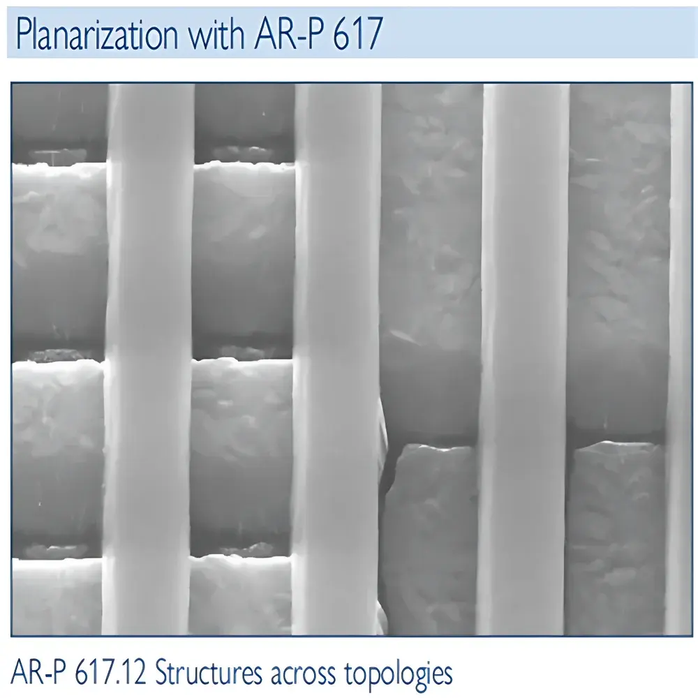
- Planarization layers in heterogeneous integration and 3D IC packaging
- Direct-write prototyping in university and industrial nanofabrication facilities
- Research applications requiring high thermal budget compatibility—e.g., post-lithography annealing, atomic layer deposition (ALD), and reactive ion etching (RIE)
FAQ
What substrates is AR-P 610 compatible with?
AR-P 610 exhibits strong adhesion to silicon, thermally grown SiO₂, fused silica, quartz, chromium, aluminum, titanium, and gold—without requiring additional adhesion promoters in most cases.
Is AR-P 610 suitable for 193 nm (ArF) lithography?
No. AR-P 610 is optimized for 248 nm (KrF) and electron-beam exposure; it lacks the transparency and acid amplification kinetics required for 193 nm immersion lithography.
How is sensitivity adjusted during processing?
Sensitivity is modulated primarily through the post-apply soft bake (PAB) step—higher temperatures (e.g., 160–180 °C) and extended durations increase deprotection efficiency and reduce required exposure dose.
Can AR-P 610 be used in high-vacuum e-beam systems?
Yes. Its low volatility and minimal residual solvent content after PAB ensure low outgassing rates, preserving column vacuum integrity and reducing contamination risk in high-resolution e-beam writers.
What developer concentration is recommended?
Standard 0.26 N tetramethylammonium hydroxide (TMAH) aqueous solution is recommended; alternative concentrations (0.13–0.40 N) may be used to fine-tune contrast and develop rate for specific feature geometries.


