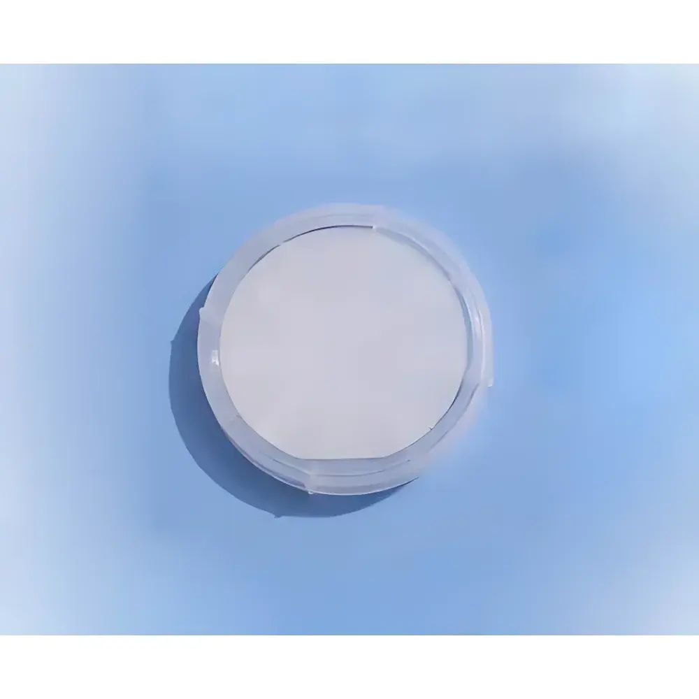
AlN Thin Film on Sapphire Substrate (KJ-ALN-SAP508)
| Brand | Hefei Kejing |
|---|---|
| Substrate Diameter | 50.8 mm ±1 mm |
| Substrate Orientation | c-plane (0001) ±1.0° |
| Substrate Material | Al₂O₃ (sapphire) |
| Film Thickness | 10–5000 nm |
| Conductivity Type | Semi-insulating |
| Threading Dislocation Density (TDD) | XRD FWHM (0002) < 500 arcsec, XRD FWHM (10–12) < 1500 arcsec |
| Effective Area | >80% |
| Surface Finish | Single-side polished |
| Customization | Available for non-standard orientations and dimensions |
| Packaging | Class 1000 cleanroom environment |
Overview
AlN thin films deposited on c-plane sapphire substrates serve as high-performance nucleation and buffer layers for the epitaxial growth of wide-bandgap semiconductors—particularly GaN-based heterostructures used in high-power, high-frequency, and optoelectronic devices. This product leverages hydride vapor phase epitaxy (HVPE) to achieve high-crystallinity aluminum nitride layers with controlled stoichiometry and low defect density. Unlike bulk AlN substrates—which remain prohibitively expensive and challenging to scale—AlN-on-sapphire templates offer a cost-effective, manufacturable alternative while preserving critical lattice-matching advantages (a-lattice mismatch ~13.8% with GaN, mitigated by strain relaxation mechanisms and interfacial dislocation filtering). The films are engineered for structural integrity, thermal stability up to 1000 °C in inert atmospheres, and compatibility with standard MOCVD and MBE reactor loading protocols.
Key Features
- High-purity AlN layer grown via HVPE on optically polished c-plane sapphire (Al₂O₃), ensuring reproducible surface morphology and minimal particulate contamination.
- Tight crystallographic control: XRD rocking curve full-width at half-maximum (FWHM) values of <500 arcsec for the (0002) reflection and <1500 arcsec for the (10–12) reflection—indicative of low threading dislocation density and superior in-plane alignment.
- Film thickness tunable from 10 nm (ultra-thin seed layer) to 5000 nm (thick buffer), with nominal 1500 nm ±10% offered as standard configuration on 2-inch (50.8 mm) wafers.
- Semi-insulating behavior enables reduced parasitic capacitance and leakage current in vertical device architectures, supporting RF and power electronics applications.
- Single-side polished substrate ensures compatibility with automated wafer handling systems and eliminates backside scattering during optical characterization (e.g., PL, Raman, ellipsometry).
- Manufactured and packaged in ISO Class 6 (1000) cleanroom environments; final storage and shipping in ISO Class 5 (100) clean bags or individual SMIF-compatible cassettes to maintain surface integrity.
Sample Compatibility & Compliance
This AlN template is validated for integration into standard III-nitride epitaxy platforms, including AIXTRON and Veeco MOCVD reactors, as well as Riber and SVT Associates MBE systems. It meets baseline requirements for semiconductor-grade substrate specifications per SEMI Standard F48-0218 (Specification for Sapphire Wafers for Epitaxial Use) and aligns with common industry acceptance criteria for buffer layer qualification in GaN-on-sapphire LED and HEMT manufacturing lines. While not certified to ISO 9001 or IATF 16949 at the wafer level, all production batches undergo in-house metrology verification—including XRD θ–2θ scans, AFM surface roughness (Ra < 0.3 nm over 5 × 5 µm), and optical inspection per MIL-STD-1246C Level C particle limits.
Software & Data Management
No embedded firmware or proprietary software is associated with this passive substrate product. However, full metrological traceability is provided with each shipment: certificate of conformance includes batch ID, deposition date, XRD FWHM data (both (0002) and (10–12)), thickness measurement method (spectroscopic ellipsometry calibrated against cross-sectional TEM), and surface inspection report. All documentation complies with GLP-aligned record retention practices, supporting audit readiness for internal quality management systems and customer-facing qualification packages. Raw XRD and ellipsometry datasets can be supplied upon request in ASCII or .csv format for integration into enterprise MES or SPC platforms.
Applications
- Buffer layer for GaN-based high-electron-mobility transistors (HEMTs) targeting 5G base station amplifiers and radar systems.
- Nucleation template for UV-A and UV-C light-emitting diodes (LEDs) requiring low-defect-density AlN underlayers to improve internal quantum efficiency.
- Substrate platform for AlGaN deep-UV photodetectors and solar-blind sensors.
- Thermal interface material test substrate in high-power packaging R&D, leveraging AlN’s high thermal conductivity (~180 W/m·K) and coefficient of thermal expansion (CTE) match with GaN.
- Reference standard for calibration of XRD texture analyzers and high-resolution transmission electron microscopy (HRTEM) sample preparation workflows.
FAQ
Is this AlN film doped or undoped?
All standard configurations are undoped, semi-insulating AlN. Intentional doping (e.g., Si, Mg, or C) is available under custom development agreements.
What is the maximum recommended annealing temperature prior to epitaxy?
Pre-growth annealing in N₂ or NH₃ ambient is supported up to 950 °C for 10 minutes without measurable film degradation or interfacial reaction.
Can you supply AlN on SiC or GaN substrates instead of sapphire?
Yes—AlN films on 4H-SiC (0001) and free-standing GaN substrates are available; lead time and minimum order quantities differ.
Do you provide cross-sectional TEM samples?
Cross-sectional TEM lamellae prepared via FIB lift-out can be supplied as an add-on service; contact technical sales for protocol alignment.
Are these wafers suitable for direct metalorganic chemical vapor deposition (MOCVD) loading without pre-treatment?
Yes—wafers are delivered oxide-free and ready for in-situ H₂/NH₃ bake; no additional RCA cleaning is required unless specified for ultra-low contamination applications.


 and Vehicle Classification System")