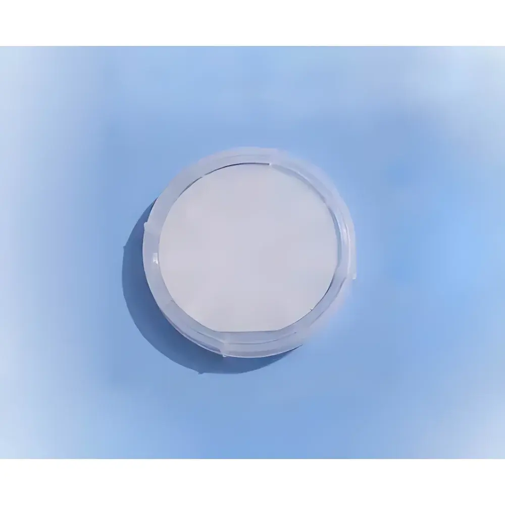
AlN Thin Film on Sapphire Substrate – Quartz Crystal Microbalance (QCM) Grade Epitaxial Template
| Brand | Hefei Kejing |
|---|---|
| Origin | Anhui, China |
| Manufacturer Type | Authorized Distributor |
| Origin Category | Domestic |
| Model | AlN-QCM-50.8mm |
| Price Range | USD 1–999 |
| Substrate | c-plane Sapphire (0001) ±1.0° |
| Diameter | 50.8 mm ±1 mm |
| Thickness | 10–5000 nm |
| Conductivity Type | Semi-Insulating |
| Dislocation Density | XRD FWHM <0002> < 500 arcsec, <10-12> < 1500 arcsec |
| Effective Area | >80% |
| Surface Finish | Single-Side Polished |
| Packaging | Class 1000 Cleanroom, Class 100 Clean Bag or Individual Cassette |
Overview
The AlN Thin Film on Sapphire Substrate is a high-purity, epitaxially grown piezoelectric template engineered for precision quartz crystal microbalance (QCM) sensor fabrication, surface acoustic wave (SAW) device development, and high-frequency resonator applications. Fabricated via hydride vapor phase epitaxy (HVPE), this AlN film exhibits superior crystalline quality, low defect density, and excellent lattice matching with c-plane sapphire (Al2O3) substrates. Its semi-insulating nature, combined with high acoustic velocity (~6,000 m/s) and temperature stability (up to 700 °C in inert atmospheres), makes it suitable for harsh-environment QCM sensing, real-time thin-film deposition monitoring, and gravimetric analysis in vacuum or controlled-gas environments. Unlike bulk AlN wafers, this epitaxial thin-film format provides cost-effective scalability while maintaining the electromechanical coupling coefficient (k2 ≈ 6–7%) required for sensitive mass-loading detection down to sub-monolayer resolution.
Key Features
- High-crystallinity AlN layer grown on optically polished c-plane sapphire (0001) ±1.0° orientation — ensuring minimal interfacial strain and acoustic loss
- Controlled thickness range from 10 nm to 5000 nm, with tight uniformity (±5% across >80% effective area) for reproducible resonance frequency tuning
- Semi-insulating electrical behavior (ρ > 1012 Ω·cm at 25 °C), enabling low-noise electrode integration and minimal dielectric loss in RF operation
- Low threading dislocation density confirmed by high-resolution XRD: FWHM of (0002) reflection < 500 arcsec; (10–12) reflection < 1500 arcsec
- Compatible with standard photolithography, lift-off, and e-beam evaporation processes — facilitating rapid prototyping of QCM electrodes (e.g., Au, Pt, Cr/Au)
- Available on alternative substrates (SiC, GaN) upon request — supporting heteroepitaxial integration for hybrid SAW/QCM platforms
Sample Compatibility & Compliance
This AlN-on-sapphire template meets baseline material specifications for ISO/IEC 17025-accredited laboratories performing QCM-based thin-film characterization. While not a finished instrument, the substrate conforms to common wafer-handling protocols in Class 1000 cleanrooms and supports ISO 14644-1 compliant packaging (Class 100 clean bags or individual SMIF-compatible cassettes). The sapphire substrate complies with ASTM F797-22 for optical-grade single-crystal alumina wafers. For regulated applications involving GLP/GMP-compliant gravimetric monitoring (e.g., pharmaceutical thin-film coating validation), users must validate film performance per USP or ISO 20523:2019 guidelines using calibrated reference standards.
Software & Data Management
As a passive sensing substrate, this AlN film does not include embedded firmware or proprietary software. However, it is fully interoperable with industry-standard QCM instrumentation platforms—including those from Q-Sense (Biolin Scientific), Stanford Research Systems (SR830 lock-in + QCM-D modules), and home-built impedance analyzers operating from 1 MHz to 100 MHz. Raw resonance data (f0, Δf, ΔD) acquired via network analyzers or phase-locked loop systems can be imported into MATLAB, Python (with SciPy/NumPy), or OriginLab for Sauerbrey mass calculation, Voigt-model viscoelastic fitting, or time-resolved adsorption kinetics analysis. Audit-trail-capable data acquisition systems compliant with FDA 21 CFR Part 11 may be used when paired with validated instrument drivers and electronic lab notebooks (ELNs).
Applications
- Development of high-stability QCM sensors for real-time monitoring of atomic layer deposition (ALD) and molecular beam epitaxy (MBE) processes
- Fabrication of temperature-compensated SAW devices for wireless gas sensing in industrial safety systems
- Substrate for epitaxial growth of GaN-based power electronics where AlN buffer layers reduce threading dislocation propagation
- Reference-grade templates for calibrating XRD rocking curves and measuring strain relaxation in III-nitride heterostructures
- Platform for studying interfacial hydration dynamics of biomolecular films (e.g., lipid bilayers, antibody monolayers) under controlled humidity
FAQ
Is this AlN film pre-patterned with electrodes?
No — this is a bare epitaxial template. Electrodes must be deposited separately via sputtering or evaporation.
Can I specify off-axis sapphire orientations (e.g., r-plane or m-plane)?
Yes — custom substrate orientations are available upon technical review and minimum order quantity agreement.
What is the typical RMS surface roughness (Ra) after polishing?
Measured Ra is ≤0.2 nm over 5×5 µm AFM scan area for standard single-side polished wafers.
Do you provide certificate of conformance or XRD reports?
Yes — CoC and full XRD ω-scans (0002 and 10–12) are included with each shipment upon request.
Is hydrogen annealing recommended prior to metal electrode deposition?
Hydrogen annealing at 800–900 °C in N2/H2 ambient is optional but improves surface stoichiometry and reduces native oxide; process parameters must be qualified per your metallization stack.


")
