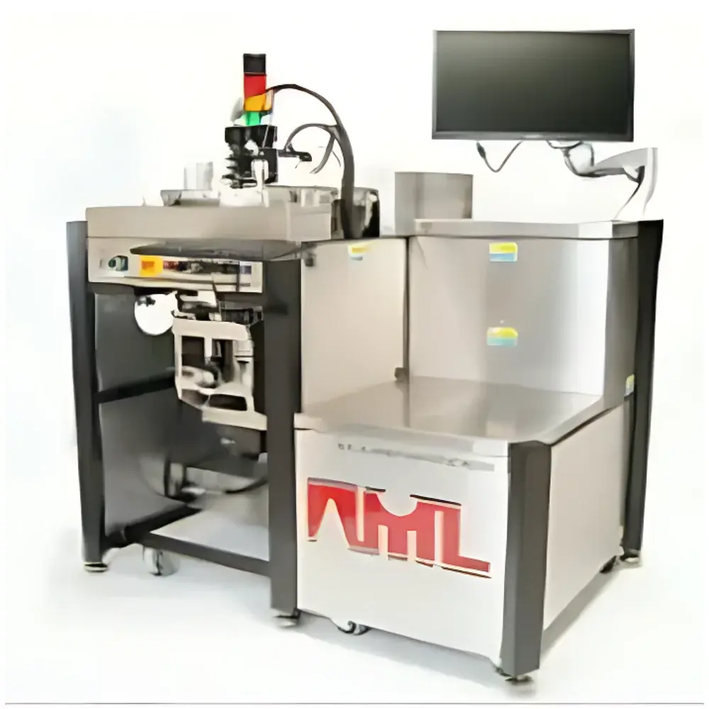

AML AWB-04 & AWB-08 Advanced Wafer Bonding Platforms
| Brand | AML |
|---|---|
| Origin | United Kingdom |
| Model | AWB-04 & AWB-08 Platform |
| Vacuum Base Pressure | ≤1×10⁻⁶ mbar |
| Maximum Bonding Force | 40 kN |
| Maximum Temperature | 560 °C |
| Anodic Bonding Voltage | 0–2.5 kV DC (up to 40 mA) |
| Alignment Accuracy | ±1 µm (in-situ, hot or cold) |
| Compatible Wafer Sizes | 2″, 3″, 4″, 5″, 6″, and 8″ |
| Bonding Environments | High vacuum, UHV (optional), controlled process gas (e.g., forming gas), or atmospheric inert gas |
| Optical System | Dual CCD microscope with through-the-lens illumination, visible + infrared imaging, real-time side-by-side wafer alignment display |
| Control Architecture | Fully automated PC-based system with recipe-driven operation, full parameter logging (voltage, current, integrated charge, temperature, pressure, force, separation, event timestamps), SPC-compliant data export, and remote diagnostic capability via secure network interface |
Overview
The AML AWB-04 and AWB-08 Advanced Wafer Bonding Platforms are precision-engineered semiconductor bonding systems designed for high-reliability, process-critical wafer-level assembly in R&D, pilot-line, and high-mix production environments. These platforms implement a unified in-situ alignment and bonding architecture based on electro-mechanical actuation, thermally stable optical metrology, and programmable environmental control. Unlike conventional bonders requiring pre-chamber alignment or manual intervention, the AWB series performs real-time, sub-micron alignment—under vacuum or process gas—at elevated temperatures (up to 560 °C) and high mechanical load (up to 40 kN). This enables direct, anodic, eutectic, glass frit, adhesive, solder, and thermo-compression bonding modalities—all within a single, validated platform. The system’s core innovation lies in its dual-platen thermal management, motorized manipulator kinematics, and synchronized force–separation–optical feedback loop, ensuring repeatable bond uniformity across 2″ to 8″ substrates while maintaining compliance with semiconductor manufacturing traceability requirements.
Key Features
- In-situ alignment with ±1 µm accuracy under operational conditions (vacuum, temperature, force), eliminating thermal drift errors via selectable hot/cold calibration modes.
- Dual independent platen temperature control (1 °C resolution), programmable heating/cooling ramps, and full-size heated electrodes for uniform anodic bonding field distribution (0–2.5 kV DC, up to 40 mA).
- Fully automated dry turbo pumping system achieving base pressures down to 1×10⁻⁶ mbar; optional ultra-high vacuum (UHV) configuration available for oxide-sensitive processes.
- Twin-CCD optical system with through-the-lens illumination, simultaneous visible and infrared imaging, and side-by-side real-time display of top/bottom wafer features—including widely spaced 3D alignment marks.
- Motorized X/Y/θ/Z manipulator enabling precise in-vacuum wafer positioning and parallelism adjustment; contact force applied via manual or motorized hydraulic actuation (max 40 kN).
- Integrated in-situ UV curing module (optional), RAD low-temperature activation tool, triple-stack bonding capability, and CMOS-compatible process chamber design.
- Comprehensive data acquisition architecture compliant with GLP/GMP principles: all parameters—including voltage, current, integrated charge, chamber pressure, temperature gradients, force profiles, wafer separation trajectories, and event logs—are timestamped, stored in standardized binary files, and exportable for SPC trend analysis.
Sample Compatibility & Compliance
The AWB-04 accommodates wafers from 3″ to 6″ and discrete chips; the AWB-08 extends support to 6″ and 8″ wafers, including non-standard substrates (e.g., rectangular dies, odd-shaped MEMS carriers) where alignment is not required. Both platforms support bonding of silicon, SOI, glass, quartz, LiNbO₃, GaAs, and thin-film metalized substrates. Process compatibility includes ASTM F1702 (anodic bonding), ISO 17025-aligned calibration protocols, and adherence to JEDEC JEP122G reliability test preparation guidelines. All electrical and vacuum subsystems meet CE Machinery Directive 2006/42/EC and Low Voltage Directive 2014/35/EU. Data integrity conforms to FDA 21 CFR Part 11 requirements when configured with electronic signature and audit trail modules.
Software & Data Management
Control is executed via AML’s proprietary BondMaster™ software suite, running on an industrial-grade Windows OS platform with deterministic real-time I/O. The interface supports both manual parameter tuning and fully automated recipe execution—including auto-deskilling sequences for production operators (e.g., “one-click” align-and-bond). Each run generates a structured .bondlog file containing raw sensor streams, derived metrics (e.g., charge accumulation rate, thermal expansion compensation offsets), and metadata (batch ID, operator ID, equipment ID, timestamped SPC flags). Files are natively compatible with MATLAB, Python (via HDF5 readers), and JMP for statistical modeling. Remote diagnostics are enabled via TLS-secured Ethernet connection, allowing AML Field Application Engineers to perform live parameter interrogation, firmware updates, and root-cause analysis without physical access.
Applications
These platforms serve critical functions in MEMS packaging (cap wafer bonding, cavity sealing), advanced image sensor fabrication (3D-stacked CIS, hybrid bonding), microfluidic device integration (glass–silicon hermetic seals), power electronics (SiC/GaN die attach), and quantum device assembly (superconducting qubit cabling, cryogenic interposer bonding). Specific use cases include formation-gas-assisted in-situ oxide reduction prior to direct bonding, low-stress anodic bonding of thin SOI membranes, and high-throughput temporary bonding/debonding for TSV processing. The 1 µm alignment stability under thermal load makes the AWB uniquely suited for heterogeneous integration involving CTE-mismatched material stacks.
FAQ
What wafer sizes does the AWB-04 support?
The AWB-04 is optimized for 3″, 4″, 5″, and 6″ wafers, as well as individual chips and non-circular substrates.
Can the AWB perform bonding under forming gas?
Yes—the system supports absolute pressure control from 1×10⁻⁶ mbar to 2 bar, enabling precise forming gas (N₂/H₂) or argon ambient delivery for surface activation and native oxide management.
Is in-situ UV curing integrated or optional?
In-situ UV curing is a factory-installed option, featuring broadband (320–405 nm) LED sources with intensity and exposure time programmability.
How is traceability ensured for regulated environments?
All bonding runs generate immutable log files with cryptographic hash signatures, supporting 21 CFR Part 11 audit trails when paired with domain-authenticated user accounts and role-based access controls.
Does the system support triple-stack bonding?
Yes—via optional triple-stack bonding tooling, enabling sequential bonding of three-layer structures (e.g., sensor–interposer–ASIC) with intermediate alignment verification.
What calibration standards apply to the 1 µm alignment specification?
Alignment accuracy is verified using NIST-traceable grating standards and interferometric reference plates, with annual recalibration recommended per ISO/IEC 17025 laboratory practice.
Related Products


