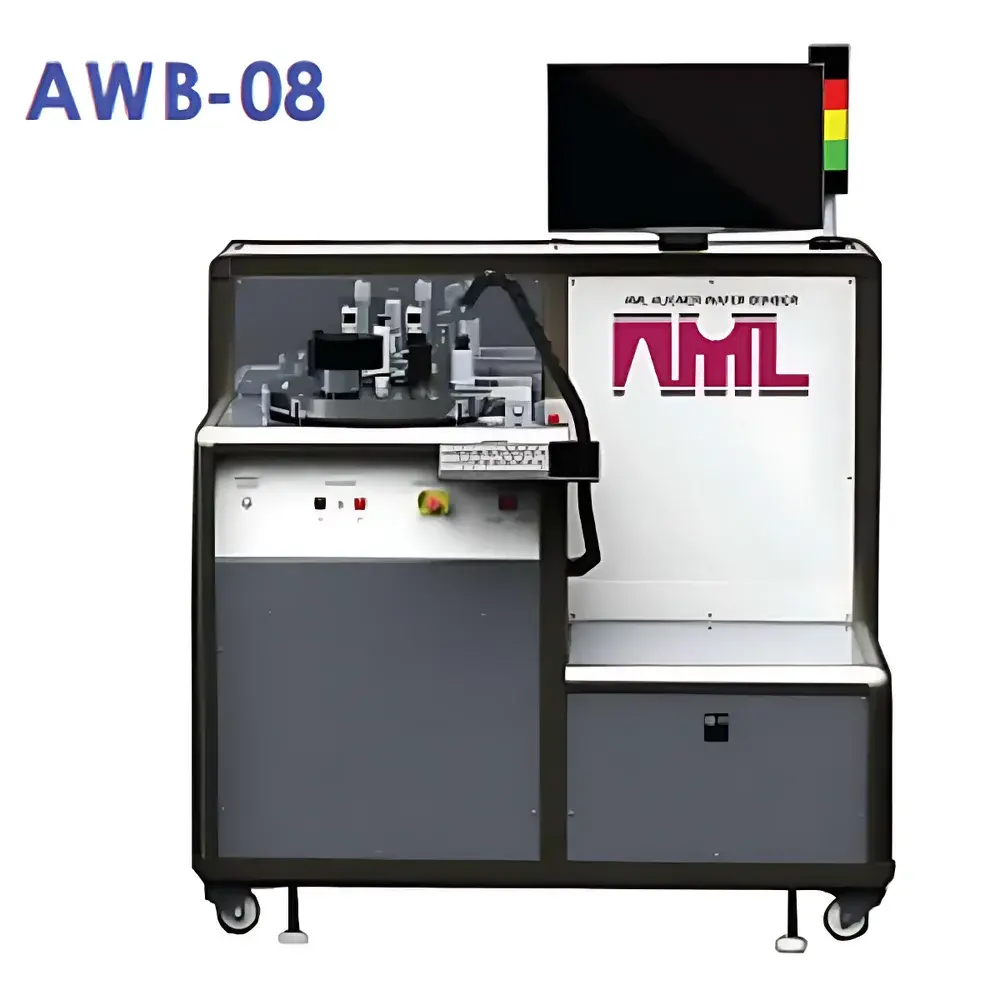
AML AWB-04 / AWB-08 / ROCK-04 / ROCK-08 In-Situ Alignment Wafer Bonding System
| Brand | AML |
|---|---|
| Origin | United Kingdom |
| Model Series | AWB-04, AWB-08, ROCK-04, ROCK-08 |
| Maximum Wafer Size | 200 mm |
| Heating Range | Up to 650 °C |
| Bonding Chamber Vacuum | ≤1 × 10⁻⁵ mbar (with turbomolecular pump) |
| Control Interface | Windows-based HMI with full process logging |
| Compliance | Designed for GLP/GMP-aligned R&D and pilot-line environments |
| Automation Level | Semi-automatic (manual load/unload, fully automated alignment, activation, and bonding) |
Overview
The AML AWB-04, AWB-08, ROCK-04, and ROCK-08 series are semi-automatic in-situ alignment wafer bonding systems engineered for high-precision, thermally driven wafer-level integration in semiconductor R&D and low-volume production. These systems implement a unified process sequence—real-time optical alignment, surface activation (e.g., plasma or thermal), and controlled bonding—within a single vacuum-compatible chamber, eliminating inter-process contamination and registration drift. Built upon AML’s proprietary dual-stage thermal architecture, each system features independently controlled upper and lower electrode heating plates with ±0.5 °C thermal uniformity across the entire 200 mm wafer area, enabling reproducible anodic, thermo-compressive, eutectic, glass-frit, direct Si–Si, and SOI bonding. The integrated nanoscale alignment stage achieves sub-100 nm overlay accuracy under vacuum conditions, supported by real-time video feedback and motorized X/Y/θ fine adjustment. As a UK-designed platform certified for ISO 9001-compliant manufacturing, the AWB/ROCK series serves as a reference-grade tool for process development requiring traceable, repeatable, and auditable bonding protocols.
Key Features
- In-situ optical alignment with live CCD imaging and automated pattern recognition for sub-micron overlay control
- Multi-mode bonding capability: anodic, thermo-compressive, eutectic, glass-frit, direct silicon, and SOI bonding—all programmable within one platform
- High-vacuum bonding chamber (≤1 × 10⁻⁵ mbar) equipped with turbomolecular pumping and bake-out functionality
- Dual-zone independent heating system (0–650 °C) with PID-controlled ramp/soak profiles and thermal uniformity <±0.5 °C over 200 mm
- Nanopositioning stage with active wedge compensation for thickness variation correction during bond force application
- Modular chamber design supporting interchangeable tooling for MEMS, microfluidics, compound semiconductors, and 3D IC applications
- Windows-based control software with full audit trail, electronic signatures, and 21 CFR Part 11–compliant data archiving options
Sample Compatibility & Compliance
The AWB/ROCK platforms accommodate wafers up to 200 mm diameter—including silicon, quartz, glass, GaAs, SiC, and thin-film metal substrates—with optional carrier handling for fragile or warped wafers. All models comply with CE marking requirements and incorporate safety interlocks per IEC 61000-6-2/6-4. Process recipes are structured to align with ASTM F2129 (for MEMS packaging reliability), ISO 14644-1 (cleanroom compatibility), and JEDEC JEP122G (failure mechanisms in bonded die stacks). For regulated environments, optional validation packages support IQ/OQ/PQ execution and GLP/GMP documentation templates.
Software & Data Management
AML’s BondMaster™ control suite provides deterministic sequencing of alignment, activation, and bonding steps with millisecond-level timing resolution. Each run logs temperature, pressure, vacuum level, alignment offset, and applied force at 10 Hz sampling rate. Data exports natively to CSV and SQLite formats; optional modules enable integration with LabArchives ELN or Siemens Opcenter Quality. Audit trails include user ID, timestamp, parameter set hash, and deviation flags—fully compliant with FDA 21 CFR Part 11 when configured with digital certificate authentication and role-based access control.
Applications
- MEMS fabrication: Hermetic encapsulation of accelerometers, gyroscopes, and resonant sensors via anodic or glass-frit bonding
- Microfluidic device assembly: Bonding of PDMS/glass/silicon layers with controlled channel integrity and surface energy tuning
- SOI substrate manufacturing: High-yield direct wafer bonding with post-bond annealing and Smart Cut™ process support
- Compound semiconductor packaging: Eutectic Au–Sn bonding for GaN HEMTs and SiC power modules
- 3D heterogeneous integration: TSV-enabled stacking with thermal budget control for copper–copper hybrid bonding development
- Nanoimprint lithography (NIL): Integrated resist curing and mold imprinting under vacuum and elevated temperature
FAQ
What wafer sizes does the AWB/ROCK series support?
Standard configurations handle 100 mm, 150 mm, and 200 mm wafers; custom chucks are available for non-standard substrates including diced dies and ceramic carriers.
Can the system perform both alignment and bonding without breaking vacuum?
Yes—the entire workflow (alignment → surface activation → bonding) occurs inside a single vacuum chamber, minimizing particle exposure and eliminating re-alignment errors.
Is process transfer possible between AWB/ROCK and higher-end AML systems?
All recipe files and thermal/pressure profiles are binary-compatible with AML’s fully automated ROCK-XL and AWB-XL platforms, enabling seamless scale-up from R&D to pilot line.
Does the system support DOE-driven process optimization?
BondMaster™ includes built-in Design of Experiments (DOE) wizards for multi-variable parameter sweeps (temperature ramp rate, dwell time, bond force gradient) with automated result correlation to overlay error and bond strength metrics.
What vacuum performance is achievable with standard configuration?
Base pressure reaches ≤5 × 10⁻⁶ mbar with optional cryo-trapping; standard turbomolecular pump achieves ≤1 × 10⁻⁵ mbar, sufficient for oxide-free anodic bonding and low-contamination eutectic processes.


