
AML AWB-04 / AWB-08 / ROCK-04 / ROCK-08 In-Situ Alignment Wafer Bonding Systems
| Brand | AML |
|---|---|
| Origin | United Kingdom |
| Model | AWB-04, AWB-08, ROCK-04, ROCK-08 |
| Application | In-situ alignment, surface activation, wafer bonding, and nanoimprint lithography (NIL) |
| Compliance | Designed for Class 100 cleanroom integration |
| Control Architecture | Motorized precision stages with sub-micron alignment repeatability |
| Vacuum Compatibility | <5×10⁻⁶ mbar base pressure |
| Thermal Bonding Range | Ambient to 500 °C |
| Alignment Accuracy | ≤±25 nm (3σ, optical auto-alignment mode) |
| NIL Capability | Compatible with rigid and soft stamps |
Overview
The AML AWB-04, AWB-08, ROCK-04, and ROCK-08 are fully integrated in-situ alignment wafer bonding platforms engineered for high-precision semiconductor process development and advanced packaging R&D. These systems implement a sequential yet co-located process flow—optical alignment, plasma or thermal surface activation, and vacuum-compatible bonding—within a single, ultra-stable vacuum chamber. Unlike conventional bonders requiring manual transfer between alignment and bonding stations, the AML platform eliminates inter-chamber contamination risk and positional drift, enabling reproducible sub-50 nm overlay accuracy across 100 mm (AWB-04/ROCK-04) and 200 mm (AWB-08/ROCK-08) wafers. The architecture is based on high-rigidity granite bases, piezo-driven fine-stage positioning, and real-time interferometric feedback for closed-loop alignment control. All models support both direct (fusion) and intermediate-layer (e.g., SiO₂, polymer, metal) bonding schemes, with programmable ramp/soak thermal profiles and active pressure control during bond formation.
Key Features
- In-situ optical alignment using high-magnification telecentric imaging and pattern recognition algorithms—no wafer repositioning required post-alignment
- Integrated RF or microwave plasma activation module (13.56 MHz or 2.45 GHz), configurable for O₂, Ar, N₂, or forming gas chemistries
- Dual-mode bonding capability: thermal compression (up to 500 °C, 10 kN max force) and anodic bonding (up to ±1.5 kV, 200 °C)
- Nanoimprint lithography extension: compatible with quartz, silicon, and PDMS stamps; supports both thermal NIL (T-NIL) and UV-curable resist processing
- Modular vacuum system with turbomolecular pumping, achieving ≤5×10⁻⁶ mbar base pressure and ≤1×10⁻⁵ mbar operating pressure during bonding
- Full software-defined process scripting: users define multi-step recipes—including alignment offset compensation, activation dwell time, ramp rates, and bond force profiling—with audit-trail logging
Sample Compatibility & Compliance
The AWB and ROCK series accommodate standard semiconductor substrates including silicon, SOI, glass, fused silica, sapphire, and compound semiconductors (GaAs, InP, SiC). Both 100 mm and 200 mm wafer formats are supported with carrier-based or edge-grip handling; optional backside infrared thermometry enables non-contact temperature monitoring during thermal cycles. All systems comply with CE machinery directive (2006/42/EC), electromagnetic compatibility (2014/30/EU), and low-voltage directive (2014/35/EU). Vacuum and plasma subsystems meet ISO 14644-1 Class 5 (ISO Class 5) cleanroom integration requirements. Process data integrity adheres to ALCOA+ principles (Attributable, Legible, Contemporaneous, Original, Accurate, Complete, Consistent, Enduring, Available), supporting GLP and GMP-aligned validation protocols.
Software & Data Management
Control is executed via AML’s proprietary BondMaster™ software suite, built on a deterministic real-time OS (QNX) with dual-redundant Ethernet interfaces. The GUI provides synchronized live viewing of alignment marks, real-time force/temperature/pressure traces, and overlay error heatmaps. All process parameters, image captures, and sensor logs are timestamped and stored in HDF5 format with SHA-256 checksums. Role-based access control (RBAC), electronic signatures, and 21 CFR Part 11-compliant audit trails are enabled by default. Export options include CSV, XML, and industry-standard SECS/GEM messaging for factory automation integration (SEMI E30, E40, E57).
Applications
These platforms serve critical functions in MEMS fabrication (e.g., cavity sealing of gyroscopes and pressure sensors), 3D IC stacking (TSV-to-TSV alignment and bonding), heterogeneous integration (Si photonics + III-V lasers), and nanoscale patterning for metasurfaces and plasmonic devices. In R&D environments, they enable rapid iteration of bonding interface engineering—evaluating interfacial energy, interdiffusion kinetics, and defect propagation under controlled atmospheres. The integrated NIL functionality supports maskless fabrication of sub-100 nm features for biosensor arrays, anti-reflective textures, and photonic crystal templates—without requiring e-beam writing infrastructure.
FAQ
What wafer sizes are supported by each model?
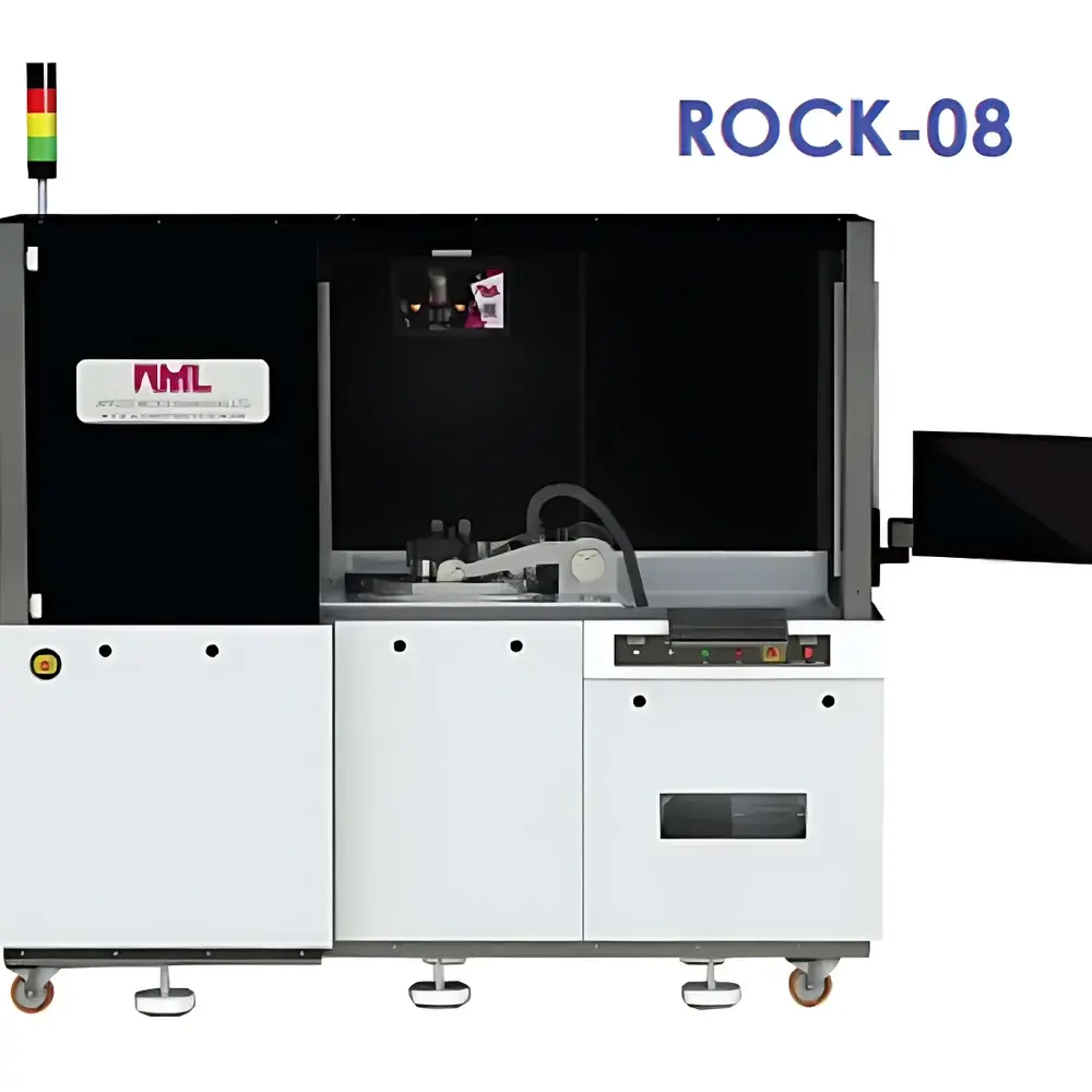
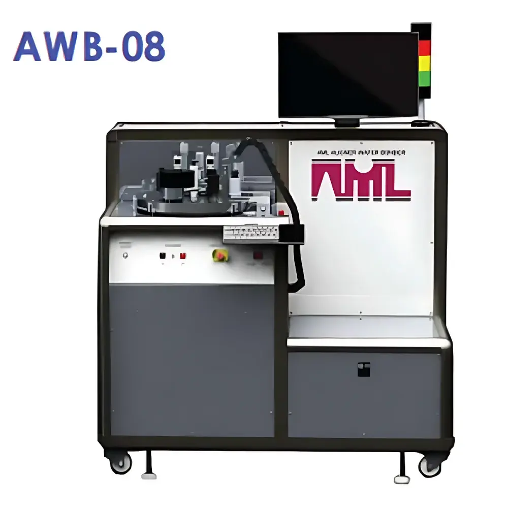
The AWB-04 and ROCK-04 are configured for 100 mm wafers; the AWB-08 and ROCK-08 support 200 mm wafers with automated cassette-to-chamber loading.
Can the system perform both front-side and back-side alignment?
Yes—dual-sided optical path design allows infrared-transparent substrate alignment (e.g., Si wafers) using backside illumination and front-side mark detection.
Is remote diagnostics and service support available?
All units include embedded Teledyne LeCroy remote debug interfaces and support secure TLS-encrypted VNC sessions for qualified AML Field Application Engineers.
How is process traceability ensured for regulated environments?
BondMaster™ implements full electronic batch records, immutable parameter logs, and user-action timestamps—all exportable in PDF/A-2b or ASAM ODS format for regulatory submission.
Are custom end-effectors or vacuum chucks available?
AML offers application-specific chuck designs (e.g., electrostatic, porous ceramic, or heated ceramic) and metrology-grade alignment mark carriers upon request.


