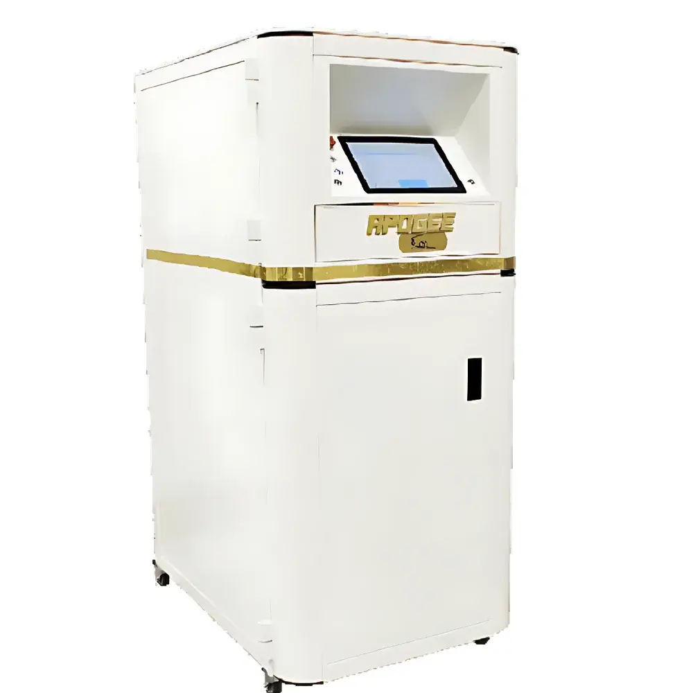
Analysis Bonder300 Semiconductor Wafer Bonding System
| Brand | Analysis |
|---|---|
| Origin | USA |
| Manufacturer Type | Authorized Distributor |
| Origin Category | Imported |
| Model | Bonder300 |
| Pricing | Available Upon Request |
Overview
The Analysis Bonder300 is a precision-engineered, semi-automated wafer bonding system designed for R&D laboratories and pilot-line semiconductor packaging operations. It implements thermocompression and anodic bonding principles—leveraging controlled thermal gradients, uniform mechanical pressure, and high-vacuum environments—to achieve void-free, high-strength interfacial adhesion between dissimilar or lattice-mismatched substrates. Unlike fully automated cluster tools, the Bonder300 delivers production-grade throughput (14–20 wafers per hour) without requiring cleanroom-integrated robotics, complex facility interfaces, or multi-million-dollar capital investment. Its architecture balances operational flexibility with process repeatability—making it ideal for compound semiconductor (SiC, GaN, GaAs, InP), MEMS, photonics, and heterogeneous integration applications where rapid process iteration and material compatibility are critical.
Key Features
- Dual-zone heated platens with independent temperature control (up to 450 °C) enable symmetric thermal ramping across both top and bottom wafers—minimizing thermal stress-induced warpage and interfacial cracking.
- Self-leveling platen mechanism compensates for total thickness variation (TTV) up to ±15 µm, ensuring uniform bond pressure distribution across 50–300 mm substrates.
- High-vacuum bonding chamber (<1 Pa base pressure) eliminates micro-voids and oxide entrapment during interface formation—critical for hermetic sealing in MEMS encapsulation and 3D IC stacking.
- Modular vacuum pre-bond separation: carrier and device wafers remain physically isolated during evacuation, preventing premature contact and surface contamination prior to controlled alignment and compression.
- Real-time multi-parameter monitoring: synchronized logging of piston force (±0.5% FS), platen temperature (±0.3 °C), chamber vacuum (±0.05 Pa), and cycle timing with 0.1-second step resolution.
Sample Compatibility & Compliance
The Bonder300 supports rigid and brittle substrate combinations including silicon, sapphire, fused silica, SiC, GaN, GaAs, and InP—enabling direct bonding, metal diffusion bonding, and glass frit processes. All wetted surfaces are constructed from ultra-low-outgassing stainless steel and ceramic-coated components compliant with SEMI F21 standards. The system meets ISO 14644-1 Class 5 cleanroom compatibility when operated inside appropriate enclosures. Process logs include full audit trails (user ID, timestamp, parameter set, hardware state) aligned with GLP and FDA 21 CFR Part 11 requirements for electronic records and signatures.
Software & Data Management
The Bonder300 runs on a Linux-based embedded control platform with a responsive 10.1-inch capacitive touchscreen HMI. Remote access is provided via HTTPS-secured web browser interface—supporting real-time monitoring, recipe editing, and event-triggered push notifications to desktop, tablet, or mobile devices. Each bonding run generates a timestamped .CSV log file containing full sensor time-series data, operator annotations, and checksum-verified configuration snapshots. Logs are exportable for offline statistical process control (SPC) analysis using JMP, Python Pandas, or MATLAB. Firmware updates and recipe libraries can be deployed over Ethernet without interrupting lab operations.
Applications
- Compound semiconductor device packaging: GaN-on-SiC power module die attach and lid sealing.
- MEMS inertial sensor vacuum cavity formation via silicon-glass anodic bonding.
- Heterogeneous integration: TSV-enabled 3D stacking of CMOS image sensors with optical substrates.
- Photonic integrated circuit (PIC) assembly: InP laser diode bonding to silicon nitride waveguide platforms.
- R&D process qualification: rapid screening of bond strength, interfacial morphology, and delamination resistance under varying temperature/pressure profiles.
FAQ
What substrate sizes does the Bonder300 support?
It accommodates wafers and substrates ranging from 50 mm to 300 mm in diameter—or equivalent rectangular formats—with full thermal and mechanical uniformity across the entire bonding area.
Can bonding recipes be transferred between multiple Bonder300 units?
Yes. Recipes—including temperature ramps, pressure profiles, vacuum sequences, and dwell times—are stored as portable XML files and can be imported/exported between systems without recalibration.
Is the system compatible with existing factory automation protocols?
The Bonder300 provides optional SECS/GEM interface support (via RS-422 or TCP/IP) for integration into MES-driven semiconductor fabs, enabling automated job dispatch and status reporting.
How is process traceability ensured for quality audits?
Every bonding cycle generates a unique digital certificate containing raw sensor data, operator credentials, environmental conditions, and cryptographic hash verification—retained for ≥12 months by default and exportable for external QA review.
What maintenance intervals are recommended for sustained >99% uptime?
Preventive maintenance is scheduled every 600 operating hours or 6,000 cycles—whichever occurs first—with field-replaceable vacuum seals, thermocouple assemblies, and load cell modules calibrated per ISO/IEC 17025-accredited procedures.


