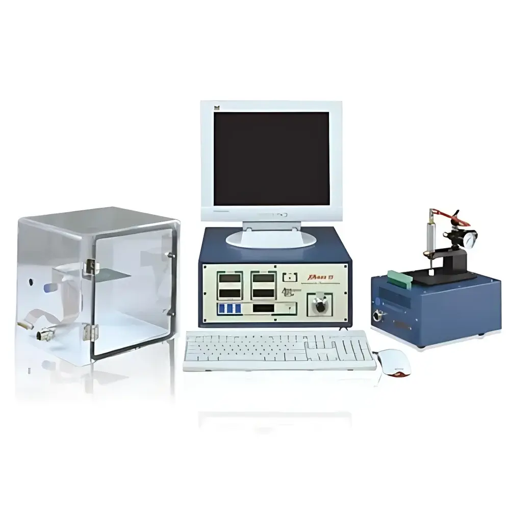
Analysis Tech PHASE12 Transient Thermal Resistance Analyzer
| Brand | Analysis Tech |
|---|---|
| Origin | USA |
| Model | PHASE12 |
| Compliance | JEDEC JESD51-1, JESD51-14, JESD51-8, JESD51-12 |
| Thermal Resolution | ±0.007°C |
| Junction Temperature Accuracy | ±0.1°C |
| Voltage Measurement Accuracy | ±0.25% (0–30 V) |
| Current Measurement Accuracy | ±0.25% |
| Sampling Rate | 1 MHz |
| Max Standard Current Output | 18 A |
| Optional High-Current Power Booster | up to 1000 A |
| Junction Sensing Current Options | 1–50 mA |
| Calibration Temperature Range | Ambient to 180°C |
| Input Power | 220 VAC, 5 A, 50/60 Hz |
Overview
The Analysis Tech PHASE12 Transient Thermal Resistance Analyzer is an engineering-grade instrument designed for high-precision, time-resolved thermal characterization of semiconductor packages and power electronic devices. It operates on the principle of electrical test-based junction temperature (Tj) measurement—leveraging the well-established voltage–temperature correlation (K-factor) of semiconductor p–n junctions under low-sensing-current conditions. By applying controlled heating current and measuring real-time forward voltage drop across the device under test (DUT), the PHASE12 calculates transient thermal impedance Zth(t) with microsecond-level temporal resolution. This enables full reconstruction of the device’s internal thermal structure function—a physics-based representation of thermal resistance (R) versus cumulative thermal capacitance (C)—in strict accordance with JEDEC JESD51-1 and JESD51-14 standards. Unlike steady-state methods, the transient approach captures dynamic heat flow through heterogeneous layers (e.g., die attach, substrate, solder, TIM, heatsink interface), making it indispensable for reliability validation, process control, and thermal design optimization in automotive, aerospace, LED, and wide-bandgap (SiC/GaN) applications.
Key Features
- Comprehensive transient thermal impedance (Zth) acquisition from 1 µs to >100 s, supporting both heating and cooling phase analysis
- Full compliance with JEDEC JESD51-1 (static/dynamic Rja, Rjc, Rjb, Rjl), JESD51-14 (structure function extraction), and JESD51-12 (ΨJB reporting guidelines)
- Integrated K-factor calibration module with ceramic-coated magnetic stirrer, thermally stable mineral oil bath (4 L), and programmable ramp control (ambient to 180°C)
- Dual-channel high-fidelity sensing: ±0.25% accuracy for voltage/current, 1 MHz sampling, and junction temperature resolution of ±0.007°C
- Multi-die thermal crosstalk analysis via matrix-based thermal resistance modeling (R11, R12, R21, R22) for stacked or parallel-die modules
- Die attachment quality evaluation through localized thermal impedance mapping at the die–substrate interface
- SOA (Safe Operating Area) and surge current testing capability with synchronized thermal-electrical stress profiling
Sample Compatibility & Compliance
The PHASE12 supports a broad range of discrete and packaged semiconductor devices—including MOSFETs, IGBTs, diodes, LEDs, and multi-die power modules—in standard JEDEC footprints (TO-220, D²PAK, QFN, LFPAK, etc.). Dedicated mechanical fixtures (JEDEC-compliant Rjc and Rjb test clamps) ensure repeatable thermal boundary conditions per JESD51-14. Optional accessories include the EVN-12 still-air test enclosure (eliminating convective artifacts per JESD51-2), calibrated wind tunnel (for forced-convection Rja validation), and high-current Power Booster units (up to 1000 A). All measurements adhere to ISO/IEC 17025 traceable calibration protocols; raw data files include full metadata (sensor IDs, timestamps, environmental conditions) to support GLP/GMP audit trails and FDA 21 CFR Part 11–compliant electronic records.
Software & Data Management
The proprietary PHASE12 Control Suite provides real-time visualization of Zth(t) curves, automatic structure function transformation (via Laplace inversion), and comparative overlay of multiple DUTs. The software implements JEDEC-recommended deconvolution algorithms to extract layer-specific R–C networks, enabling quantitative assessment of interfacial defects (e.g., voids in die attach) and thermal bottlenecks. Export formats include CSV, MATLAB (.mat), and PDF reports with embedded calibration certificates. Data integrity is enforced through role-based user access, cryptographic audit logs, and version-controlled analysis workflows—fully aligned with laboratory information management system (LIMS) integration requirements. All firmware and analysis modules undergo annual verification against NIST-traceable thermal reference standards.
Applications
The PHASE12 serves as a core metrology tool in semiconductor qualification labs, packaging R&D centers, and failure analysis facilities. Typical use cases include: validating thermal interface material (TIM) performance under power cycling; benchmarking die-attach process consistency across wafer lots; diagnosing thermal degradation mechanisms in SiC MOSFETs after HTGB testing; optimizing LED package architecture using structure function bottleneck identification; and generating JEDEC-compliant thermal datasheets for customer-facing documentation. Its ability to resolve sub-millisecond thermal transients makes it uniquely suited for characterizing ultrafast switching devices where traditional IR thermography lacks temporal resolution.
FAQ
What standards does the PHASE12 comply with?
It fully implements JEDEC JESD51-1 (transient thermal impedance), JESD51-14 (structure function analysis), JESD51-8 and JESD51-12 (Ψ-parameter reporting), and supports ASTM E1461 (laser flash) cross-validation protocols.
Can the PHASE12 measure thermal resistance of multi-die packages?
Yes—it performs coupled thermal resistance matrix analysis (Rij) for up to eight dies using independent heating and sensing channels, enabling crosstalk quantification and individual die thermal budget allocation.
How is junction temperature calibrated?
Via the integrated mineral oil bath (JESD51-5 compliant), which establishes the device-specific K-factor (dVf/dT) over ambient–180°C using T-type thermocouples and low-sensing-current (<50 mA) bias conditions.
Is software validation available for regulated environments?
Yes—the Control Suite includes IQ/OQ documentation templates, 21 CFR Part 11 audit trail configuration, and third-party validation support for GxP-compliant laboratories.
What is the minimum detectable thermal resistance increment?
With ±0.007°C temperature resolution and 1 MHz sampling, the system resolves thermal resistance changes below 0.01°C/W for typical power devices operating above 1 W.


