Angstrom Sciences HiPIMS Magnetron Sputtering System
| Brand | Angstrom Sciences |
|---|---|
| Origin | USA |
| Manufacturer Type | Authorized Distributor |
| Origin Category | Imported |
| Model | HiPIMS |
| Pricing | Upon Request |
Overview
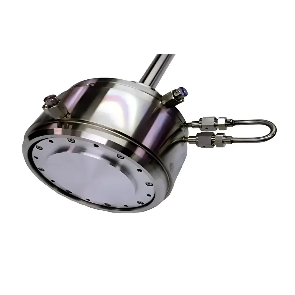
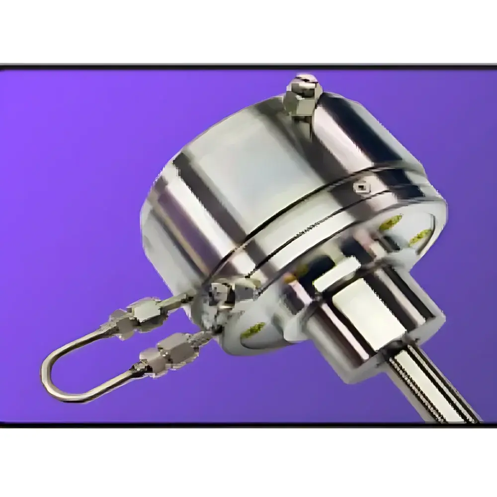
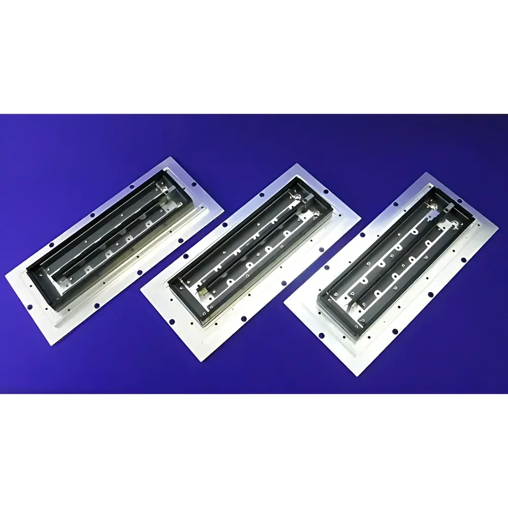
The Angstrom Sciences HiPIMS Magnetron Sputtering System is an advanced pulsed direct-current (DC) magnetron sputtering platform engineered for high-ionization physical vapor deposition (PVD). Unlike conventional DC or RF sputtering, High-Power Impulse Magnetron Sputtering (HiPIMS) delivers ultra-high peak power densities—typically in the range of kW/cm²—with low average power, enabling exceptional ionization fractions (>50% for many metals) of the sputtered flux. This results in superior film density, enhanced adhesion, reduced columnar growth, and improved stoichiometry control—particularly critical for complex oxides, nitrides, and nanolaminated structures. The system integrates configurable magnetic circuit architectures—supporting both discrete field tuning via interchangeable internal magnet arrays and continuous field modulation through external magnet height adjustment—optimized for circular and linear cathode geometries. Designed for R&D and pilot-scale thin-film fabrication, it serves as a core tool for functional coatings in microelectronics, optical interference stacks, wear-resistant tribological layers, and barrier films for flexible electronics.
Key Features
- HiPIMS-specific pulse generator with adjustable pulse width (20–200 µs), frequency (50–1000 Hz), and peak power up to 3 kW per cathode channel
- Modular magnetron design accommodating both circular (2″, 3″, 4″, 6″) and linear cathodes with field-tunable configurations
- Interchangeable internal magnet assemblies for discrete magnetic field profiling (e.g., standard, high-confinement, uniform-field variants)
- Externally mounted magnet positioning system enabling real-time, motorized adjustment of magnetic pole height for continuous B-field optimization
- Integrated vacuum interlock and plasma emission monitoring (OES-ready interface) for process reproducibility
- Water-cooled cathode housing with thermal management rated for sustained HiPIMS operation at >10⁶ pulses/hour duty cycle
- Compliant with SEMI S2-0201 safety standards and CE-marked for industrial laboratory use
Sample Compatibility & Compliance
The HiPIMS system supports substrate sizes up to 200 mm diameter (standard configuration), with optional expansion to 300 mm wafers or custom fixtures for irregular geometries—including foils, fibers, and 3D components. It accommodates substrates ranging from silicon wafers and fused silica to stainless steel, titanium alloys, and polymer films (with temperature-controlled stage option: −100 °C to 500 °C). Process compatibility extends across metallic targets (Al, Ti, Cr, Cu, Ta), compound ceramics (Al₂O₃, TiO₂, ZrO₂), and reactive co-sputtering setups using MFC-controlled Ar/O₂/N₂ gas mixing. All hardware and control firmware comply with ISO 9001:2015 manufacturing protocols and support GLP/GMP documentation requirements—including audit trails, user access levels, and electronic signature capability when paired with optional compliance software modules.
Software & Data Management
Operation is managed via Angstrom Sciences’ proprietary PlasmaLink™ v4.2 control suite, running on a real-time Windows-based industrial PC. The software provides synchronized waveform logging (pulse voltage/current/pressure), automated recipe storage with version control, and OES spectral acquisition (200–800 nm, 0.1 nm resolution) for endpoint detection and plasma diagnostics. Data export conforms to ASTM E1392-22 (Standard Practice for Digital Data Exchange in Thin-Film Deposition) and supports CSV, HDF5, and .tdms formats. Optional FDA 21 CFR Part 11 compliance package includes role-based authentication, electronic signatures, and immutable audit logs for regulated environments such as medical device coating development or semiconductor qualification labs.
Applications
- High-density dielectric barrier layers for MEMS encapsulation and OLED moisture protection
- TiN, CrN, and AlTiN hard coatings for precision cutting tools and aerospace components
- Transparent conductive oxides (e.g., ITO, AZO) with tunable carrier mobility for touch sensors
- Functional oxide thin films (LiCoO₂, VO₂) for solid-state battery electrodes and smart windows
- Adhesion-promoting interlayers (e.g., Ti, Cr) prior to e-beam evaporation or ALD cycles
- Surface functionalization of biomedical implants via nanostructured hydroxyapatite or Ag-doped CaP coatings
FAQ
What distinguishes HiPIMS from conventional magnetron sputtering?
HiPIMS operates with short, high-power pulses that generate dense plasma and significantly increase the ionization fraction of sputtered species—enabling superior film densification, step coverage, and interface control compared to continuous DC or RF sputtering.
Can the system be integrated into an existing UHV cluster tool?
Yes—the HiPIMS cathode module features CF-100 or ISO-K 250 flange interfaces and is compatible with standard UHV pumping systems (cryo + turbomolecular), with bake-out tolerance up to 150 °C.
Is remote diagnostics and service support available?
All systems include embedded Ethernet connectivity and optional Angstrom Remote Assist (ARA) protocol for secure, encrypted technician access to controller diagnostics and waveform analysis without compromising network security.
Does Angstrom Sciences provide target bonding and cathode refurbishment services?
Yes—certified target bonding (indium, tin, and epoxy-free diffusion bonding), cathode re-magnetization, and full rebuild services are offered under ISO 17025-accredited calibration and traceability protocols.


