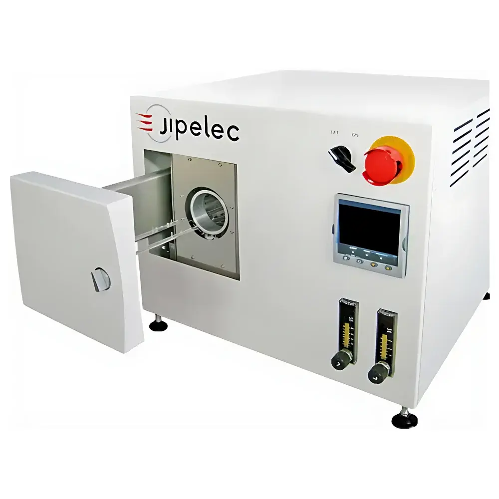
Annealsys JetLight High-Vacuum Rapid Thermal Annealing Furnace
| Brand | Annealsys |
|---|---|
| Origin | France |
| Model | JetLight |
| Instrument Type | High-Vacuum Rapid Thermal Annealing Furnace |
| Sample Size | Up to 3-inch (76 mm) diameter wafers |
| Temperature Range | Ambient to 1450 °C |
| Max Heating Rate | 150 °C/s |
| Max Cooling Rate | 200 °C/s |
| Temperature Accuracy | ±1 °C |
| Temperature Uniformity | ±1% across wafer surface |
| Vacuum Capability | Compatible with turbomolecular pumping systems |
| Control Interface | Ethernet-connected PC-based software with programmable ramp/soak profiles |
| Chamber Design | Dual-chamber option available |
| Heating Source | Array of IR halogen lamps with power-controlled (not voltage-controlled) regulation |
| Cooling Method | Forced-air cooling (low-noise, no compressed air required) |
| Chamber Material | Quartz tube within double-walled stainless-steel cold-wall structure with water-cooled jacket |
| Thermocouple Configuration | Dual N-type thermocouples — center and edge mounted for direct wafer-temperature feedback |
| Gas Handling | Up to 3 process gases with digital mass flow controllers (MFCs) and precision needle valves |
| Optional Accessories | SiC-coated graphite susceptor, high-vacuum turbomolecular pump, dual-chamber configuration |
Overview
The Annealsys JetLight is a high-precision, high-vacuum rapid thermal annealing (RTA) furnace engineered for semiconductor research and advanced materials development. It employs a tightly controlled infrared (IR) halogen lamp array to deliver localized, transient thermal energy to substrates—enabling millisecond-to-second scale thermal processing under inert, reactive, or ultra-high vacuum (UHV) environments. Unlike conventional tube furnaces, the JetLight utilizes a cold-wall quartz chamber design, where only the sample and susceptor are heated, minimizing thermal mass and enabling exceptional heating and cooling dynamics (up to 150 °C/s heating, 200 °C/s cooling). Its architecture supports both atmospheric and vacuum-based processes, making it suitable for rapid thermal oxidation (RTO), rapid thermal nitridation (RTN), ion implant activation, ohmic contact formation, and graphene synthesis via rapid thermal chemical vapor deposition (RTCVD). The system’s temperature accuracy (±1 °C) and uniformity (±1% across wafer surface) are maintained through real-time, dual-point N-type thermocouple feedback and adaptive digital PID control—ensuring reproducible thermal cycles critical for device-level process qualification.
Key Features
- Infrared halogen lamp array with power-based (not voltage-based) intensity regulation—eliminates drift from filament aging and ensures long-term thermal reproducibility.
- Cold-wall quartz chamber with integrated water-cooled stainless-steel jacket—provides zero thermal memory, high process repeatability, and rapid cooldown without residual heat soak.
- Dual N-type thermocouples mounted at wafer center and edge—enabling closed-loop temperature monitoring directly at the sample plane, not just in the chamber ambient.
- Forced-air cooling system—operates at low acoustic noise (<65 dB(A)) and requires no external compressed air infrastructure.
- Ethernet-enabled PC control interface—supports fully programmable multi-step thermal profiles with ramp, soak, and hold segments; data logging at 100 Hz resolution.
- Modular gas delivery subsystem—equipped with up to three digitally controlled mass flow controllers (MFCs), precision needle valves, and dedicated inlet nozzles positioned flush with wafer surface to eliminate cold spots and ensure laminar, uniform gas exposure.
- Optional dual-chamber configuration—physically isolates pre-treatment, annealing, and post-annealing steps to prevent cross-contamination between process sequences—essential for high-purity compound semiconductor or MEMS fabrication workflows.
- Compatibility with turbomolecular pumping systems—enables base pressures down to 1×10⁻⁷ mbar, supporting UHV-compatible annealing protocols per ASTM F1498 and ISO 14644-1 Class 4 cleanroom integration requirements.
Sample Compatibility & Compliance
The JetLight accommodates substrates up to 3-inch (76 mm) diameter—including silicon, SiC, GaN, sapphire, quartz, and flexible metal foils. Its quartz chamber geometry and optimized lamp-susceptor alignment ensure uniform irradiance distribution across standard semiconductor wafer formats. The system complies with CE marking directives (2014/30/EU EMC, 2014/35/EU LVD) and meets electrical safety standards IEC 61000-6-2/6-4. For regulated environments, optional audit-trail-enabled software modules support 21 CFR Part 11 compliance (electronic signatures, change history, user access controls), facilitating GLP/GMP-aligned R&D documentation in university cleanrooms, foundry pilot lines, and industrial process development labs.
Software & Data Management
The JetLight is operated via Annealsys’ proprietary RTAControl™ software—a Windows-based application communicating over TCP/IP Ethernet. It provides full parameter scripting, real-time temperature waveform visualization, and synchronized acquisition of thermocouple, MFC, pressure, and lamp power signals. All thermal cycles are timestamped and stored in HDF5 format, ensuring compatibility with MATLAB, Python (h5py), and LabVIEW for downstream statistical process control (SPC) analysis. Version-controlled recipe libraries allow secure sharing across multi-user lab networks, while encrypted backup archives meet institutional data retention policies.
Applications
- Rapid thermal annealing (RTA) of ion-implanted Si, Ge, and III–V layers for dopant activation.
- Ohmic contact formation on AlGaN/GaN HEMTs and Ti/Al/Ni/Au metallization stacks.
- Rapid thermal oxidation (RTO) of ultrathin gate oxides (≤2 nm) with precise thickness control.
- Rapid thermal nitridation (RTN) for SiON interfacial layer engineering.
- Graphene growth via rapid thermal CVD using CH₄/H₂ on Cu/Ni foils.
- Post-deposition annealing of high-k dielectrics (HfO₂, Al₂O₃) and ferroelectric oxides (Hf₀.₅Zr₀.₅O₂).
- Thermal budget optimization studies for CMOS scaling nodes (e.g., sub-5 nm logic, 3D NAND channel annealing).
FAQ
What vacuum level can the JetLight achieve with optional turbomolecular pumping?
With a certified 300 L/s turbomolecular pump and cryo-assisted roughing, the system reaches a base pressure of ≤1×10⁻⁷ mbar—sufficient for oxide-free annealing of reactive metals and native oxide suppression on III–V surfaces.
Is the temperature uniformity validated per SEMI standard?
Yes—uniformity mapping is performed per SEMI F13–1202 using calibrated thin-film thermocouples across a full 3-inch Si wafer; results are supplied in the factory acceptance test (FAT) report.
Can the JetLight be integrated into an automated cluster tool environment?
Via RS-232 and Ethernet APIs, the system supports SECS/GEM communication protocols and can be interfaced with MES systems for traceable lot processing in pilot-line settings.
Does the dual-chamber configuration require additional footprint or utility connections?
The dual-chamber variant uses a shared power supply, cooling circuit, and control rack—the only incremental requirement is a 300 mm extension in depth (total footprint: 700 × 1000 × 1825 mm); no additional electrical or water connections are needed.
Are calibration certificates provided for thermocouples and MFCs?
Each system ships with NIST-traceable calibration certificates for all installed N-type thermocouples and digital MFCs, valid for 12 months from commissioning.


