ANRIC AT650/850P Benchtop Plasma-Enhanced Atomic Layer Deposition System
| Brand | ANRIC |
|---|---|
| Origin | USA |
| Manufacturer Type | Authorized Distributor |
| Origin Category | Imported |
| Model | AT650/850P |
| Pricing | Upon Request |
Overview
The ANRIC AT650/850P is a compact, benchtop plasma-enhanced atomic layer deposition (PE-ALD) system engineered for precision thin-film synthesis in R&D and pilot-scale semiconductor process development. Unlike thermal ALD, this system leverages low-damage, high-density plasma generated via a remote 300 W hollow-cathode source coupled with a 60 MHz RF generator — enabling enhanced surface reactivity while minimizing ion-induced substrate damage and oxygen contamination. Its warm-wall aluminum chamber architecture supports precise thermal control of both substrate and precursor delivery lines, facilitating conformal, stoichiometrically tunable films — including metal oxides (e.g., Al₂O₃, HfO₂), nitrides (e.g., TiN, TaN), and ternary compounds — on wafers up to 150 mm (6-inch) diameter. Designed for integration into Class 100–1000 cleanrooms, the system operates under full hardware and software interlocks, ensuring safe multi-user operation and compliance with standard laboratory safety protocols.
Key Features
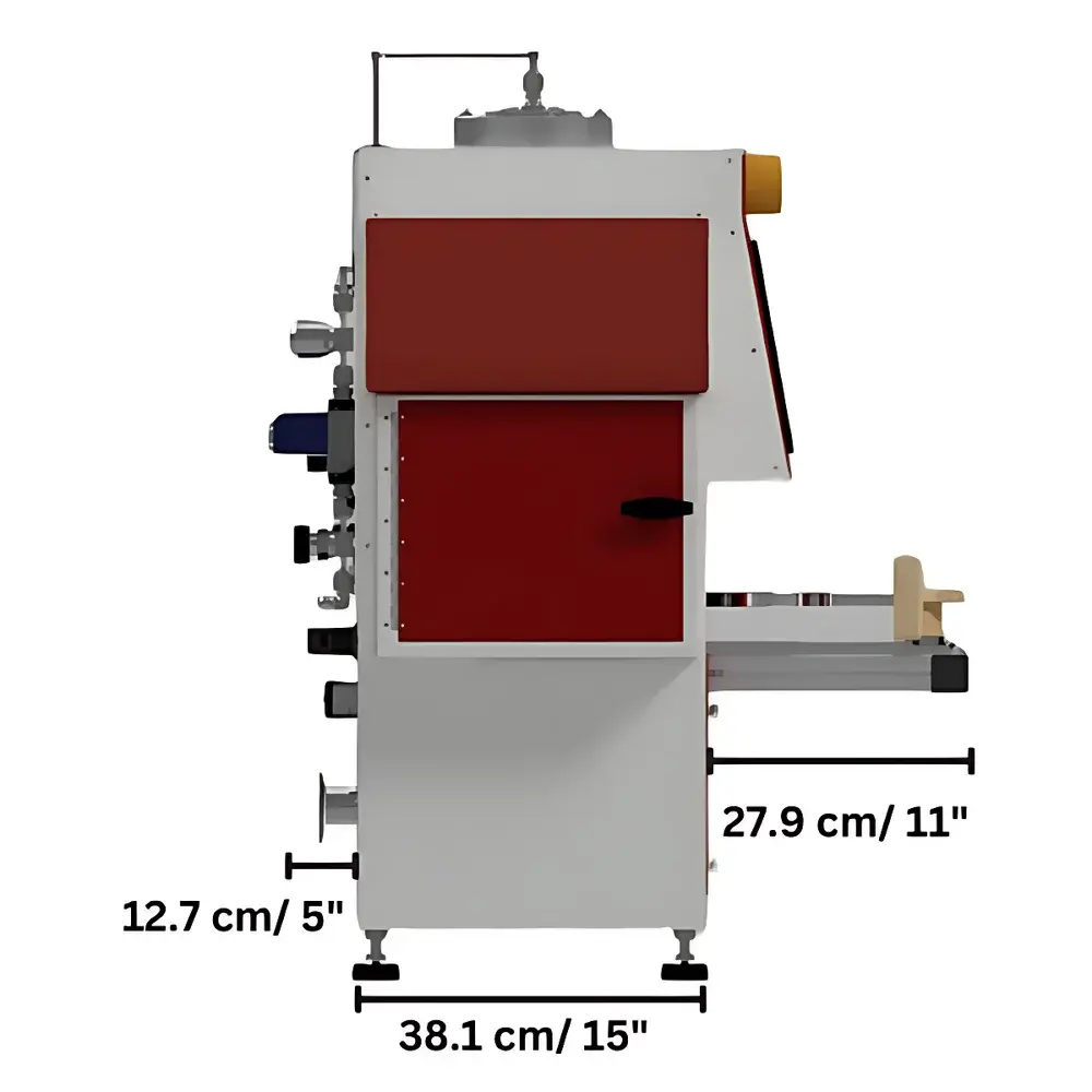
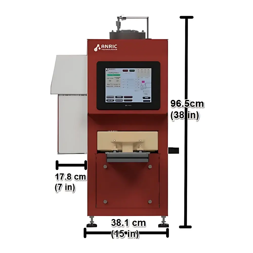
- Benchtop footprint: 38.1 cm × 38.1 cm (15″ × 15″), optimized for space-constrained labs and glovebox-compatible configurations
- Remote plasma source: 300 W hollow-cathode discharge with 60 MHz RF excitation, delivering high electron density (>10¹¹ cm⁻³) and low ion energy (<5 eV), critical for sensitive substrates and low-thermal-budget processes
- Heated sample stage: temperature range 40–400 °C (±1 °C stability); optional upgrade to 500 °C for high-activation ALD chemistries
- Precursor delivery: four independently heated metalorganic precursor lines (RT–180 °C ±2 °C, jacketed lines), plus up to four oxidant/reductant lines with ultra-fast mass flow controllers (MFCs)
- High-speed ALD valve system: plasma-compatible, high-temperature pulse valves with sub-100 ms actuation time and integrated inert gas purging for minimal cross-contamination
- Static-mode processing capability: enables uniform high-exposure plasma treatment for deep trench and high-aspect-ratio feature coverage
- Integrated PLC-based HMI: 10-inch touchscreen interface with real-time process monitoring, recipe-driven automation, and audit-trail-ready logging
Sample Compatibility & Compliance
The AT650/850P accommodates substrates up to 150 mm in diameter, with customizable electrostatic or mechanical chucks available upon request. Chamber geometry and gas dynamics are validated for uniform film growth across full wafers, as confirmed by in situ QCM (optional) and ex situ ellipsometry/XPS characterization. The system meets standard vacuum and gas-handling requirements for semiconductor tool integration: UHP N₂ purge (>99.9995% purity, 10–30 psi via VCR fittings), CDA supply (1–4 psi), and dry/wet vacuum pumping (≥19.5 cfm wet pump with PTFE-compatible fluid; NW40/NW50 exhaust interfaces). All electrical, pneumatic, and vacuum subsystems comply with CE, UL 61010-1, and ISO 14644-1 cleanroom compatibility guidelines. Software logs support GLP/GMP-aligned data integrity per FDA 21 CFR Part 11 when paired with external validation packages.
Software & Data Management
The embedded control system features a deterministic PLC platform with deterministic cycle timing and programmable logic for sub-cycle-level sequencing (e.g., precursor dose → purge → plasma exposure → purge). Preloaded recipe library includes validated processes for Al₂O₃, TiO₂, SiO₂, and TiN, with parameter traceability down to individual pulse durations and temperatures. Custom recipe entry supports complex multi-step sequences — including nanolaminates, doped layers, and ternary compositions — with independent setpoints for each precursor, plasma step, and thermal zone. All process events, sensor readings (temperature, pressure, MFC flow), and operator actions are timestamped and stored locally with export capability to CSV or SQLite. Remote operation is supported via Ethernet-connected PC interface using secure TCP/IP protocol; no cloud dependency or third-party telemetry.
Applications
- Development of high-κ dielectrics and diffusion barriers for advanced CMOS and memory devices
- Conformal coating of MEMS/NEMS structures, nanoporous templates, and vertical nanowire arrays
- Synthesis of catalytically active oxide/nitride overlayers for electrochemical and sensing applications
- Surface functionalization of 2D materials (e.g., graphene, MoS₂) with atomic-scale thickness control
- Low-temperature PE-ALD of Li-ion battery cathode coatings (e.g., AlPO₄, LiAlO₂) on NMC and LFP particles
- Process qualification and transfer to production tools via scalable, repeatable recipes
FAQ
What plasma sources are compatible with the AT650/850P?
The system integrates a proprietary remote 300 W hollow-cathode plasma source operating at 60 MHz, optimized for low-damage, high-efficiency dissociation of O₂, N₂, NH₃, and H₂.
Can the system deposit ternary or doped films?
Yes — the software supports multi-precursor pulsing sequences with independent temperature and timing control, enabling nanolaminates, doped layers (e.g., Al-doped ZnO), and ternary oxides (e.g., ZnSnO₃).
Is the system suitable for high-aspect-ratio (HAR) structures?
The static-mode plasma exposure mode, combined with ultra-fast valve response and low-pressure operation, ensures effective radical penetration into trenches >20:1 AR.
What level of process repeatability can be expected?
Typical film thickness uniformity is ≤±1.5% (1σ) across 150 mm wafers under controlled ambient conditions; growth per cycle (GPC) reproducibility is maintained within ±2% over 50+ consecutive runs.
Does the system support automated recipe transfer to production-scale tools?
Yes — all process parameters (temperatures, pulse widths, flows, plasma power) are fully exportable and documented in SI units, aligning with industry-standard process transfer protocols used by major ALD OEMs.


