Anton Paar TriTec NST³ Nano Scratch Tester
| Brand | Anton Paar TriTec (formerly CSM Instruments, Switzerland) |
|---|---|
| Origin | Switzerland |
| Model | NST³ |
| Instrument Type | Nano Scratch Tester |
| Application Scope | Thin film and coating adhesion, cohesion, scratch resistance, and mechanical integrity assessment for layers < 1 µm thick |
| Key Measurement Capabilities | Critical load (Lc) determination, real-time scratch depth profiling, friction force mapping, elastic recovery quantification, and simultaneous panoramic imaging |
Overview
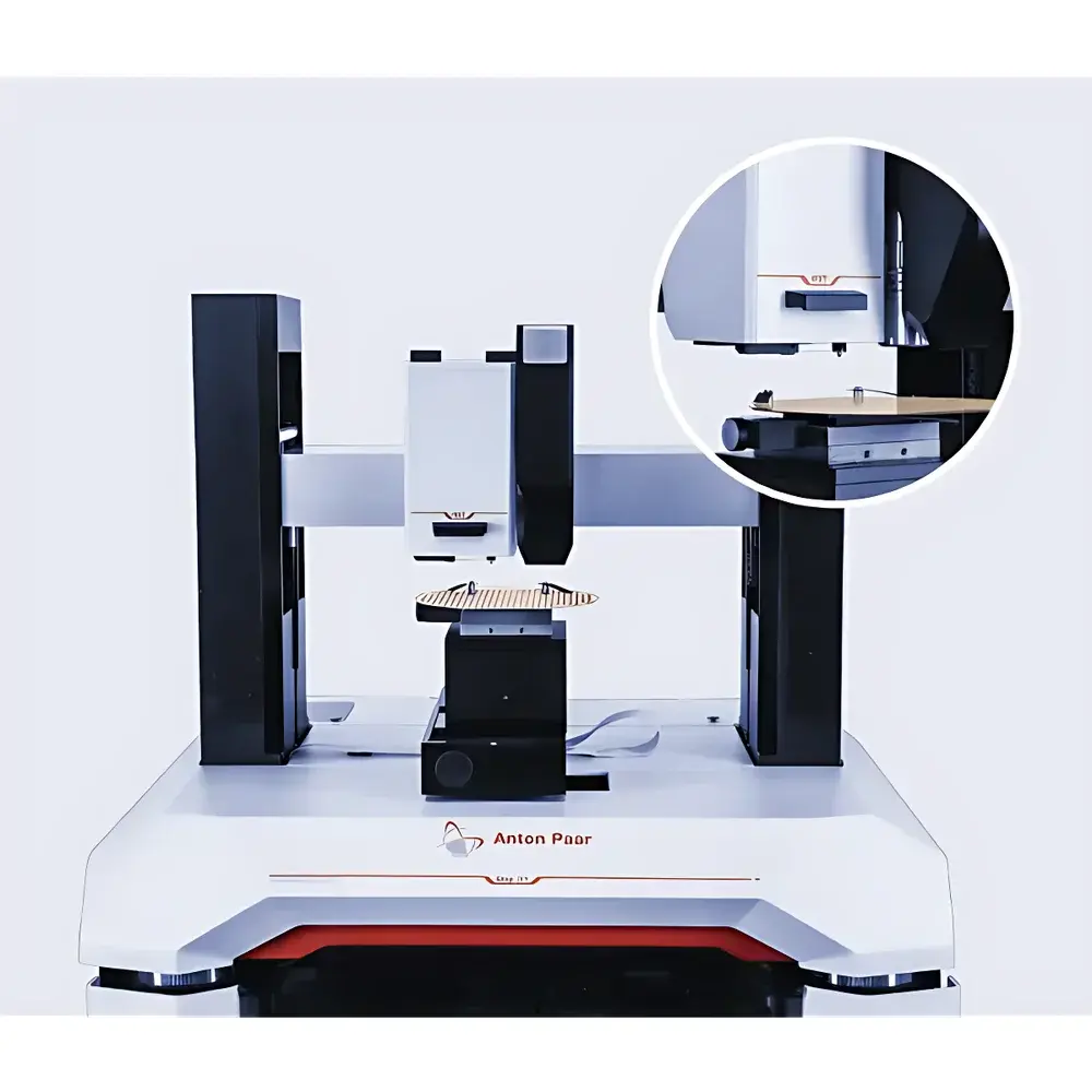
The Anton Paar TriTec NST³ Nano Scratch Tester is a high-precision, research-grade instrument engineered for quantitative mechanical characterization of ultra-thin films and functional coatings with thicknesses below 1 µm. Operating on the principle of controlled quasi-static progressive loading combined with real-time multi-sensor feedback, the NST³ applies a diamond stylus (typically Rockwell C or Berkovich geometry) to the sample surface under precisely regulated normal force while traversing at constant or variable velocity. Simultaneous acquisition of normal load, tangential friction force, vertical displacement (penetration depth), and lateral acoustic emission enables comprehensive failure mode identification—including interfacial delamination, cohesive cracking, plastic pile-up, and elastic rebound. Designed and manufactured in Switzerland, the system meets stringent metrological requirements for nanomechanical testing in academic laboratories, R&D centers, and industrial QC environments where traceable, repeatable, and standards-compliant data are essential.
Key Features
- Patented synchronized panoramic imaging: Integrated high-resolution optical microscope captures full-length scratch tracks in situ, enabling direct correlation between topographic features and mechanical response signals.
- True real-time scratch depth measurement: Dual-sensor architecture—comprising a high-stiffness piezoelectric actuator and independent displacement transducer—delivers sub-nanometer vertical resolution and eliminates thermal drift artifacts common in single-sensor systems.
- Active force feedback control: Closed-loop load regulation ensures constant-force or linear-ramp loading profiles with < ±0.5% deviation, even on non-planar, curved, or textured substrates.
- Automated critical load (Lc) detection: Multi-parameter algorithm evaluates abrupt changes in friction coefficient, acoustic emission burst intensity, and depth discontinuity to objectively identify onset of coating failure without user bias.
- Modular probe compatibility: Supports interchangeable diamond tips (e.g., sphero-conical, conical, Rockwell C) and optional environmental modules (humidity-controlled chamber, temperature stage from –30 °C to +200 °C).
Sample Compatibility & Compliance
The NST³ accommodates rigid and semi-rigid substrates including silicon wafers, optical glasses, metallic alloys (e.g., stainless steel, Ti-6Al-4V), ceramic tiles, and polymer films mounted on stiff carriers. Sample dimensions range from 10 × 10 mm to Ø150 mm, with maximum height of 50 mm. All test protocols align with internationally recognized standards including ISO 20502 (Thin films — Determination of adhesion by scratch testing), ASTM C1624 (Standard Test Method for Adhesion Strength and Mechanical Failure Modes of Ceramic Coatings by Scratch Testing), and VDI 3822 Part 2 (Mechanical surface properties). Data audit trails comply with GLP and GMP documentation requirements; optional software modules support 21 CFR Part 11–compliant electronic signatures and secure user access levels.
Software & Data Management
Control and analysis are performed via the proprietary iNano software platform, which provides intuitive workflow-driven test setup, real-time signal visualization (load, friction, depth, AE), and post-test parametric mapping. Raw data are stored in vendor-neutral HDF5 format with embedded metadata (timestamp, operator ID, calibration history, environmental conditions). Batch processing supports statistical comparison across multiple samples, while export options include CSV, MATLAB .mat, and image sequences (TIFF/AVI) for integration into third-party analysis pipelines. Software validation documentation (IQ/OQ/PQ) is available upon request for regulated industries.
Applications
- Adhesion evaluation of PVD/CVD hard coatings (TiN, CrN, DLC) on cutting tools and biomedical implants.
- Mechanical reliability screening of anti-reflective, hydrophobic, and barrier coatings on display glass and flexible electronics.
- Development and qualification of low-k dielectrics and encapsulation layers in semiconductor packaging.
- Quantitative comparison of cross-link density and network stability in UV-curable polymer films.
- Correlation of scratch resistance with deposition parameters (bias voltage, temperature, precursor flow) in plasma-enhanced ALD processes.
FAQ
What is the minimum detectable critical load (Lc) resolution?
The NST³ achieves Lc detection sensitivity down to 0.1 mN under standard operating conditions, dependent on tip geometry, coating thickness, and substrate modulus.
Can the NST³ perform tests in ambient air only, or are inert/vacuum environments supported?
Standard configuration operates in ambient laboratory air; optional glovebox-integrated or vacuum-compatible stages (10⁻³ mbar) are available for oxidation-sensitive or volatile samples.
Is calibration traceable to national metrology institutes?
Yes—force and displacement sensors are calibrated annually using NIST-traceable reference standards; calibration certificates include uncertainty budgets per ISO/IEC 17025.
How does the NST³ differentiate between adhesive and cohesive failure modes?
Through synchronized analysis of friction coefficient inflection, acoustic emission spectral signature (e.g., broadband vs. resonant peaks), and post-test SEM/FIB cross-section correlation—not inferred solely from depth discontinuity.
Does the system support automated multi-point testing across wafer-scale samples?
Yes—integrated motorized XYZ stage with pattern-based scripting enables unattended grid mapping (e.g., 5 × 5 arrays) with automatic focus and probe repositioning between locations.


