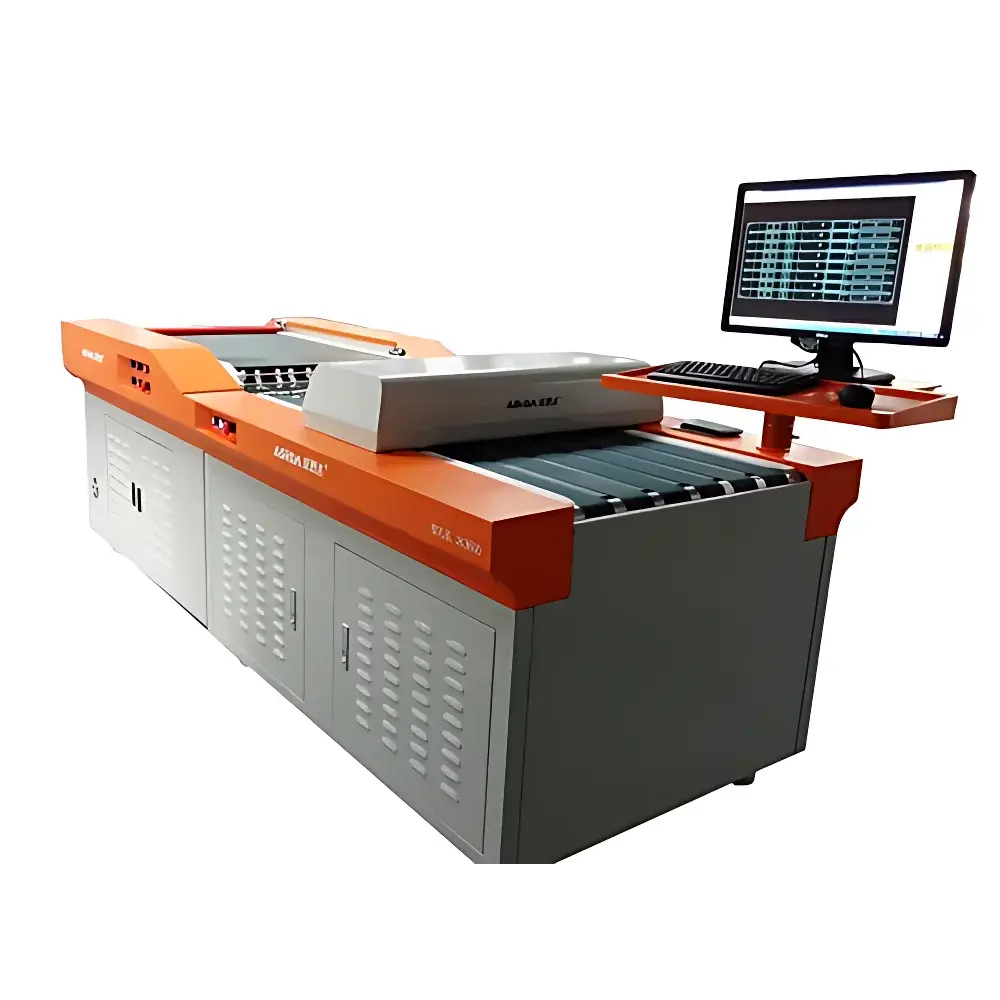
Asada JK3600 PCB Hole Inspection System
| Brand | Asada |
|---|---|
| Origin | Guangdong, China |
| Manufacturer Type | Authorized Distributor |
| Country of Origin | China |
| Model | JK3600 |
| Pricing | Available Upon Request |
| Detectable Hole Diameter Range | 0.15–10 mm |
| PCB Size Capacity | 100 × 150 mm to 630 × 650 mm |
| PCB Thickness Range | 0.3–10 mm |
| Max. Hole Count per Board | 150,000 |
| Inspection Speed | 3.5–12.5 m/min (adjustable) |
| Hole Position Repeatability | ±40 µm |
| Hole Dimension Tolerance | ±40 µm |
| Minimum Hole-to-Hole Edge Distance | 0.15 mm |
| Detection Method | Contact Image Sensor (CIS) Proximity Imaging |
| Light Source | Diffuse Long-Strip LED Array |
| Power Supply | AC 220 V, 50 Hz |
| Machine Dimensions (L×W×H) | 3550 × 1200 × 1100 mm |
| Compressed Air Requirement | 0.5–0.7 MPa |
| Weight | 450 kg |
Overview
The Asada JK3600 PCB Hole Inspection System is an automated optical inspection platform engineered for high-throughput, non-contact verification of drilled hole geometry and placement on rigid printed circuit boards (PCBs). It operates on the principle of CIS (Contact Image Sensor) proximity imaging—where a linear sensor array scans the board surface at sub-millimeter standoff distance, capturing high-resolution grayscale profiles of each drilled feature. Unlike laser triangulation or shadow-based methods, CIS enables consistent illumination and minimal parallax error across variable board thicknesses (0.3–10 mm), making it especially suitable for post-drilling, pre-packaging quality gate applications in mass-production environments. The system is calibrated to detect holes ranging from 0.15 mm to 10 mm in diameter, with positional repeatability of ±40 µm and dimensional tolerance control aligned with IPC-A-600 and IPC-6012 Class 2/3 requirements. Designed for small-format PCBs (minimum 100 × 150 mm), the JK3600 supports inline integration into final test and packaging lines where throughput—up to 12.5 meters per minute—is critical.
Key Features
- Hexa-channel parallel inspection architecture: Six independent CIS modules operate simultaneously, enabling concurrent evaluation of up to six PCBs per cycle without mechanical indexing delays.
- Wide-angle placement tolerance: Boards may be loaded within ±30° angular deviation from nominal orientation; onboard vision alignment corrects rotational offset prior to measurement, eliminating manual fixturing.
- Long-life diffuse LED illumination: Uniform, low-heat strip lighting ensures stable contrast across copper-clad, solder-masked, and bare FR-4 substrates—minimizing reflectivity-induced false calls on plated through-holes (PTH) and microvias.
- Real-time OK/NG binning logic: Integrated pneumatic diverters route boards to designated output chutes based on configurable pass/fail thresholds—including hole count, diameter deviation, plugging detection (via contrast gradient analysis), and minimum edge clearance (≥0.15 mm).
- Networked diagnostics station: Ethernet-enabled host interface allows up to eight remote workstations to access synchronized NG logs, annotated defect maps, and timestamped inspection records—facilitating root-cause analysis without interrupting line operation.
- Firmware-upgradable architecture: Field-deployable software updates support new rule sets (e.g., IPC-7351-compliant padstack validation) and calibration compensation routines via secure HTTPS upload—no hardware modification required.
Sample Compatibility & Compliance
The JK3600 accommodates standard rigid PCB materials including FR-4, polyimide, and metal-core laminates, with thicknesses spanning 0.3 mm (flex-rigid hybrids) to 10 mm (high-power modules). Its CIS optics maintain focus stability across this range without Z-axis recalibration. All measurements adhere to ISO/IEC 17025 traceable procedures; factory calibration certificates include NIST-traceable step gauges for hole diameter and position verification. The system meets CE electromagnetic compatibility (EMC) Directive 2014/30/EU and carries RoHS 2011/65/EU compliance documentation. For regulated manufacturing environments, audit trails—including user login sessions, parameter changes, and rejection event timestamps—can be exported in CSV or XML format to satisfy FDA 21 CFR Part 11 electronic record requirements when paired with validated IT infrastructure.
Software & Data Management
The proprietary Asada VisionSuite™ v4.2 provides a role-based GUI with three permission tiers: Operator (run-time control only), Technician (calibration and recipe management), and Administrator (user access policy and data export configuration). Inspection recipes store board-specific parameters—hole count expectations, diameter tolerances, exclusion zones (e.g., tooling holes), and plugging sensitivity thresholds—as XML files with SHA-256 checksums to prevent unauthorized tampering. All image data is stored locally on RAID-1 mirrored SSDs; raw CIS frames are retained for 72 hours before automatic compression to lossless PNG. Statistical process control (SPC) dashboards display real-time Cp/Cpk indices for hole diameter distribution, trend charts for misregistration drift, and Pareto analysis of defect categories (missing hole, oversized, plugged, misdrilled). Data export supports OPC UA connectivity for MES integration and ODBC drivers for direct SQL database ingestion.
Applications
- Final QA gate for consumer electronics PCBs: Verifies hole integrity after drilling and before solder mask application or component assembly.
- Automotive Tier-1 supplier audits: Confirms compliance with IATF 16949 clause 8.6.2 (release of products and services) via documented zero-defect sampling at defined AQL levels.
- LED module substrate inspection: Detects microvia blockage and annular ring consistency on aluminum-core boards used in high-lumen lighting arrays.
- Medical device PCB release: Supports GLP-aligned documentation packages by generating per-board PDF reports with embedded digital signatures and revision-controlled inspection criteria.
- Contract manufacturer yield analysis: Aggregates multi-shift defect data to identify drill bit wear patterns, feed-rate anomalies, or fixture slippage trends across production lots.
FAQ
What standards does the JK3600 use for hole diameter measurement accuracy?
The system’s ±40 µm repeatability is verified per ISO 10360-2 using certified gauge blocks traceable to NIST SRM 2192. Measurement uncertainty budgets account for thermal drift, CIS pixel pitch error, and lens distortion—fully documented in the supplied calibration report.
Can the JK3600 inspect PCBs with solder paste or conformal coating applied?
No. The CIS proximity method requires optically accessible hole interiors. Boards must be clean and dry; residual flux or uncured coating causes specular reflection artifacts that impair diameter quantification.
Is offline programming supported for new board designs?
Yes. CAD data import (Gerber RS-274X, ODB++, or IPC-2581) auto-generates inspection templates, including fiducial alignment points and expected hole lists—with manual override capability for engineering change orders.
How is air pressure regulated for the six-channel sorting mechanism?
An integrated pressure manifold with dual-stage filtration (coalescing + activated carbon) and proportional solenoid valves maintains 0.5–0.7 MPa across all six pneumatic actuators, with real-time PSI monitoring logged in the SPC dashboard.
Does the system support statistical process control (SPC) charting natively?
Yes. X-bar/R charts, Cpk trend plots, and defect-type Pareto diagrams update dynamically during inspection; historical data can be exported to Minitab or JMP via standardized .csv schema.
Related Products


