ASD JG15/JG16 UV Laser Cutting System for Flexible Printed Circuits (FPC) and Coverlay Films
| Brand | ASD (Zhengye Technology) |
|---|---|
| Origin | Guangdong, China |
| Manufacturer Type | Direct Manufacturer |
| Instrument Type | Precision UV Laser Cutting System |
| Laser Source | Solid-State UV Laser, 355 nm, 10 W |
| Max. Working Area | 610 mm × 500 mm (24″ × 18″) |
| XY Stage Max. Speed | 50 m/min |
| Positioning Accuracy | ±3 µm |
| Repeatability | ±1 µm |
| System Processing Accuracy | ±20 µm |
| Galvo Scan Range | 50 mm × 50 mm |
| Max. Material Thickness | <1 mm |
| Power Supply | AC 220 V / 50 Hz / 2.2 kW or 3-phase 380 V / 50 Hz / 5.5 kW |
| Dust Extraction Requirement | 516 m³/h |
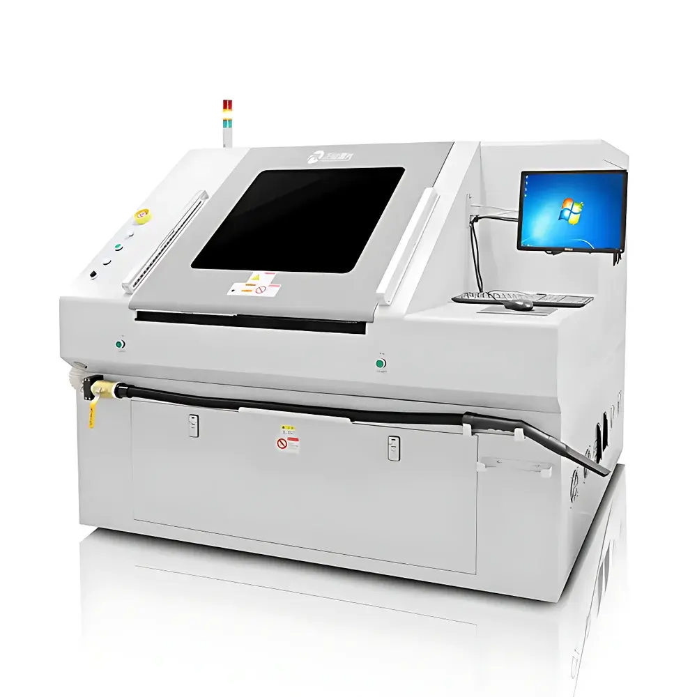
| Dimensions (L×W×H) | 1818 mm × 2317 mm × 1550 mm |
| Weight | 3500 kg |
| Operating Environment | 20 °C ±2 °C, RH <60% (non-condensing), Floor Vibration Amplitude <5 µm, Acceleration <0.05 g, Load Capacity ≥2200 kgf/m² |
Overview
The ASD JG15/JG16 UV Laser Cutting System is an industrial-grade, computer-controlled precision machining platform engineered specifically for the high-accuracy contour cutting of flexible printed circuits (FPC), coverlay films (CVL), radio-frequency (RF) substrates, and thin multilayer laminates. Unlike mechanical or CO₂ laser systems, this system employs a solid-state ultraviolet (UV) laser source operating at 355 nm wavelength—a regime where photon energy exceeds the bond dissociation energy of organic polymers and polyimide-based substrates. This enables cold ablation: material removal occurs primarily through photochemical decomposition rather than thermal melting, minimizing heat-affected zones (HAZ), eliminating delamination, suppressing burr formation, and preserving edge verticality and surface integrity. Designed for R&D laboratories, pilot production lines, and quality assurance departments in PCB and advanced packaging facilities, the system delivers deterministic, repeatable, and traceable micro-machining performance without requiring physical tooling or sacrificial fixturing.
Key Features
- Proprietary ASD control software with intuitive GUI, supporting direct import of Gerber, CAD DXF, and standard G-code files—enabling rapid job setup and geometry validation.
- Vacuum-based sample immobilization eliminates need for mechanical clamps, molds, or protective backing plates—reducing setup time and preventing substrate distortion during processing.
- Integrated optical path optimization ensures diffraction-limited beam quality, achieving sub-20 µm focused spot size and enabling fine-feature resolution down to 25 µm line width.
- Real-time auto-alignment and board-thickness measurement with dynamic Z-axis compensation—ensuring consistent focus depth and uniform cut quality across variable stack-ups.
- Multi-board nesting capability with automatic registration mark detection and global coordinate mapping—supporting batch processing of heterogeneous FPC arrays on a single substrate sheet.
- Full-axis motion control via industrial-grade motion controller and embedded IPC with 17″ display, SSD storage ≥300 GB, and deterministic real-time kernel for synchronized galvo-scanner and XY-stage coordination.
Sample Compatibility & Compliance
The JG15/JG16 system processes a broad range of thin-film substrates used in flexible electronics manufacturing, including polyimide (PI), polyester (PET), liquid crystal polymer (LCP), copper-clad laminates, solder masks, and dielectric coverlays. It also accommodates rigid substrates such as silicon wafers, alumina ceramics, and fused silica—provided thickness remains below 1 mm. All operational parameters—including laser pulse energy, scan velocity, hatch spacing, and layer-by-layer ablation depth—are programmable and auditable. The system architecture supports GLP/GMP-aligned workflows: event logs, user authentication, parameter change history, and electronic signatures are retained in accordance with FDA 21 CFR Part 11 requirements when deployed with validated software configuration. Compliance with IEC 60825-1 (laser safety), ISO 13849-1 (functional safety), and CE machinery directives is maintained through integrated interlocks, Class 1 enclosure design, and certified exhaust integration.
Software & Data Management
ASD’s proprietary FPC-Cut Suite provides full lifecycle management—from design import and simulation to process optimization and post-processing analytics. The software implements closed-loop feedback using integrated CCD vision for fiducial alignment and real-time feature verification. Cut paths are automatically optimized for minimal thermal accumulation and maximum throughput; multi-layer jobs support independent parameter sets per layer (e.g., different power levels for PI vs. copper etch). All processing data—including timestamped job logs, laser energy profiles, stage position traces, and environmental sensor readings (temperature, humidity)—are stored in structured SQLite databases with export capability to CSV, XML, or industry-standard MES-compatible formats. Audit trails comply with ISO/IEC 17025 documentation requirements for accredited testing laboratories.
Applications
This system serves critical functions in pre-production prototyping, failure analysis sample preparation, and low-volume functional testing of flexible interconnects. Typical use cases include: singulation of FPC test coupons for peel strength and bend-cycle evaluation; precise aperture cutting in coverlay films prior to selective plating; trimming of antenna patterns on RF-flex modules; isolation of sensor traces on wearable electronics substrates; and clean-edge dicing of hybrid organic-inorganic laminates for MEMS packaging qualification. Its ability to maintain dimensional fidelity under varying ambient conditions makes it suitable for metrology-grade sample prep in ISO 17025-accredited labs performing IPC-TM-650 compliant measurements.
FAQ
What file formats does the system accept for job programming?
Gerber RS-274X, CAD DXF (2D), and standard G-code (ISO 6983) are natively supported. No third-party CAM software is required for basic contour cutting.
Is vacuum chuck compatibility available for non-standard substrate sizes or thicknesses?
Yes—the vacuum table features modular sealing zones and adjustable pressure zones, accommodating substrates from 50 mm × 50 mm up to full 610 mm × 500 mm format, with thickness ranging from 25 µm to 900 µm.
How is laser focus maintained across large-area processing?
An autofocus module continuously monitors substrate height via capacitive sensing and dynamically adjusts the Z-axis position with ±0.5 µm resolution, compensating for warpage and thermal drift.
Does the system support automated optical inspection (AOI) integration?
The platform includes Ethernet/IP and Modbus TCP interfaces for seamless integration with external AOI stations or factory MES systems for closed-loop quality feedback.
What maintenance intervals are recommended for the UV laser source?
The solid-state UV laser has a rated lifetime of ≥20,000 hours under nominal operating conditions. Preventive maintenance—including optics cleaning, galvo calibration, and vacuum filter replacement—is scheduled every 500 operational hours per OEM guidelines.


