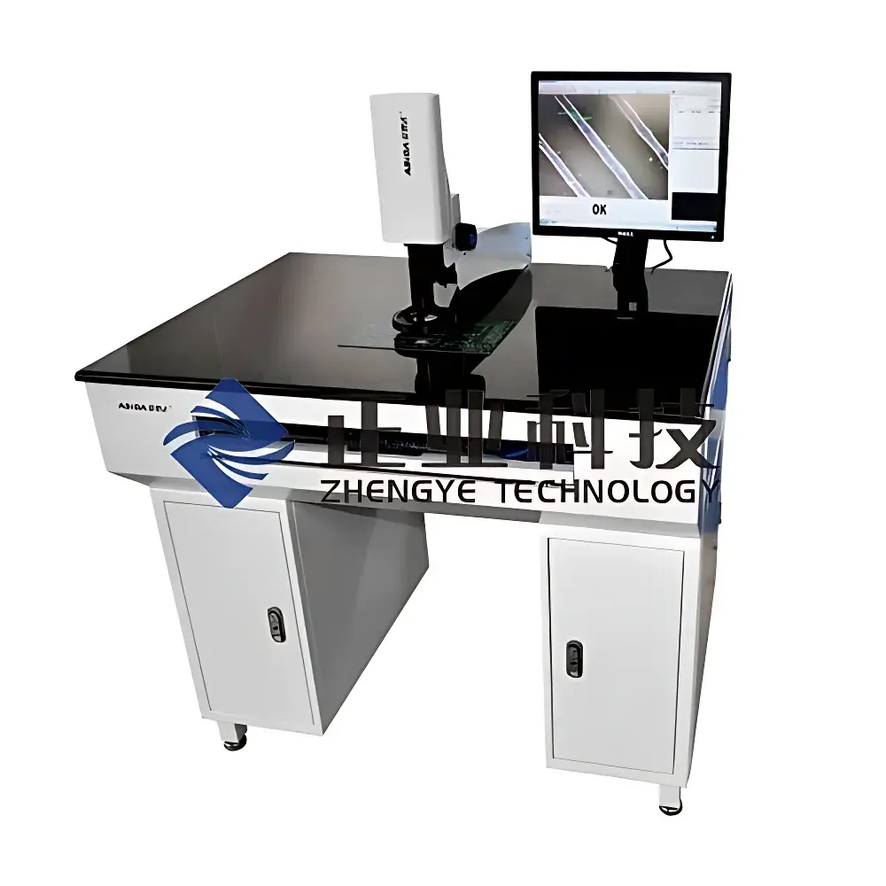
Asida XK Series PCB Trace Width & Spacing Measurement System
| Brand | Asida |
|---|---|
| Origin | Guangdong, China |
| Manufacturer Type | Authorized Distributor |
| Origin Category | Domestic (China-made) |
| Model | XK Series |
| Pricing | Available Upon Request |
| Measurement Accuracy | ±1 µm |
| Pixel Resolution | XK16/XK22: 0.70–5.20 µm/pixel |
| XK23 | 0.4–2.6 µm/pixel |
| Total Optical Magnification | 70×–450× |
| Objective Magnification | 1.4×–9× (continuous) |
| Maximum Board Width | ≤760 mm |
| Field of View | 0.53×0.4 mm to 3.4×2.5 mm |
| Minimum Measurable Line Width | ≥20 µm |
| Instrument Dimensions (w/o PC) | XK16: 135×135×310 mm |
| XK22 | 960×700×1280 mm |
| XK23 | 960×780×1280 mm |
| Weight | XK16: 1.52 kg |
| XK22 | 145 kg |
| XK23 | 190 kg |
Overview
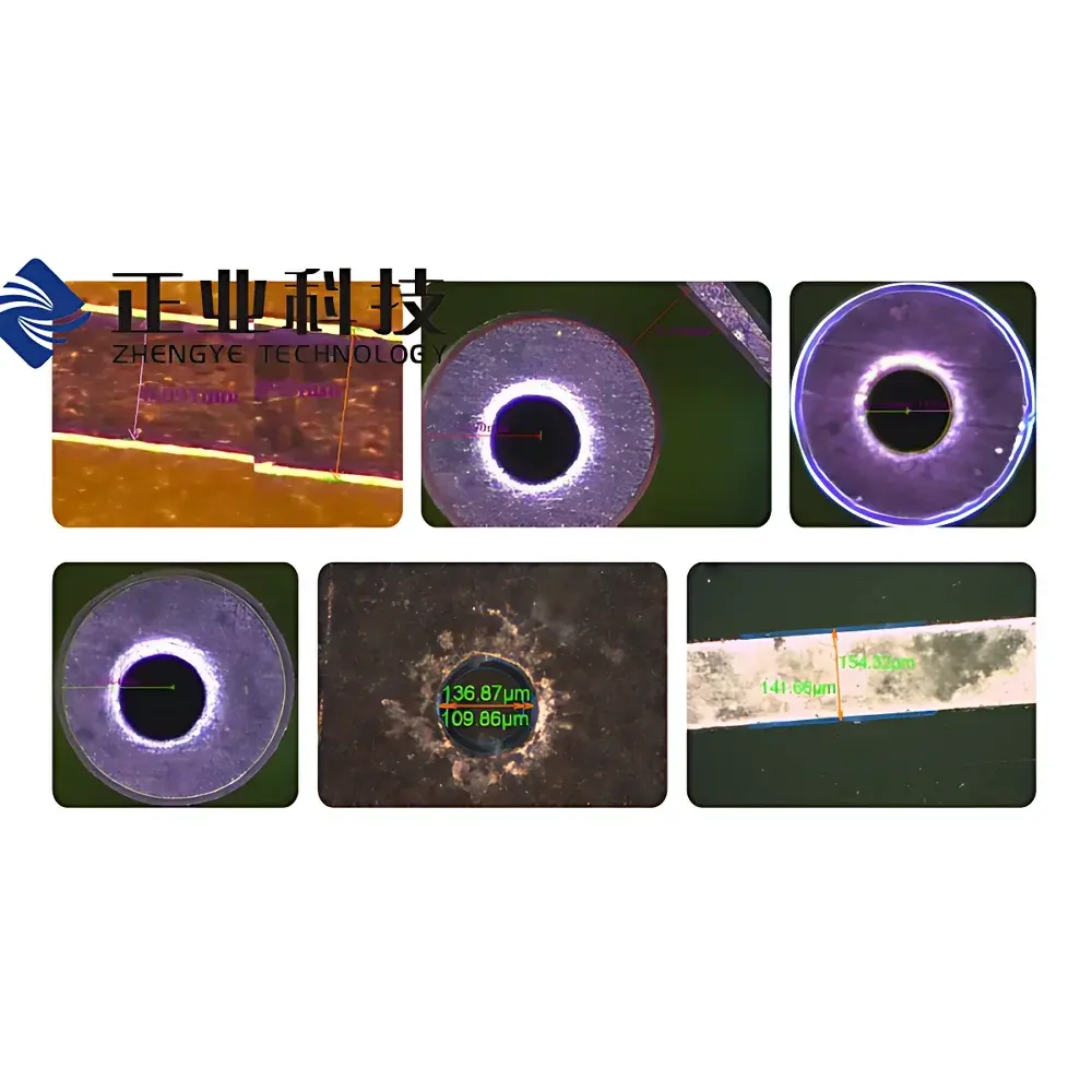
The Asida XK Series PCB Trace Width & Spacing Measurement System is a high-precision optical metrology platform engineered for non-contact, two-dimensional dimensional analysis of printed circuit board (PCB) features. It operates on the principle of digital image-based edge detection using calibrated monochrome red LED illumination and high-resolution CMOS imaging sensors. The system employs sub-pixel interpolation algorithms and automated edge localization to quantify trace widths, spacing between conductive features (e.g., line-to-line, pad-to-trace, via-to-copper), hole diameters (including blind and through-holes), arc radii, and contour geometry. Designed for integration into PCB fabrication QA/QC workflows, it supports both rigid and flexible printed circuit boards (FPCs), as well as semiconductor wafers, thin-film photomasks, and microelectronic substrates requiring micron-level feature verification. Its modular architecture allows configuration scaling—from compact benchtop units (XK16) to full-automated inline-capable systems (XK23)—while maintaining traceable measurement uncertainty aligned with ISO/IEC 17025–compliant calibration practices.
Key Features
- Precision mechanical focusing mechanism with motorized Z-axis control and fine-tuning capability for optimal depth-of-field across varying substrate topographies.
- Red LED coaxial illumination system optimized for high-contrast edge rendering on copper-clad laminates, minimizing glare and specular reflection artifacts.
- Sub-pixel edge detection algorithm enabling resolution beyond native sensor pixel pitch—achieving effective measurement resolution down to 0.4 µm/pixel (XK23 model).
- Automated feature recognition engine capable of batch-processing multiple measurement points per field of view, including parallel line pairs, circular apertures, and curved contours.
- Integrated SPC (Statistical Process Control) module compliant with AIAG SPC guidelines, supporting real-time X̄-R charting, Cp/Cpk calculation, and out-of-control condition alerts based on user-defined tolerance bands.
- Modular optical path design accommodating interchangeable objectives (1.4×–9× continuous zoom) and optional telecentric lenses for low-distortion wide-field metrology.
Sample Compatibility & Compliance
The XK Series accommodates PCB substrates up to 760 mm in width and supports standard FR-4, polyimide (FPC), ceramic, and metal-core laminates. Measurement validity is maintained across surface finishes including ENIG, HASL, OSP, and immersion silver. All models comply with IEC 61188-5-1 (Test Methods for Printed Boards – Dimensional Measurements) and reference ASTM D3593 (Standard Test Method for Measuring Dimensions of Printed Wiring Board Features). Calibration certificates are issued per ISO/IEC 17025 requirements by CNAS-accredited laboratories. For regulated environments, the system supports audit-ready data logging with time-stamped operator ID, instrument configuration metadata, and raw image archiving—enabling alignment with FDA 21 CFR Part 11 electronic record integrity expectations when deployed under GLP or GMP frameworks.
Software & Data Management
The proprietary Asida VisionMetro software suite provides a Windows-based GUI with dual-mode operation: manual point-and-measure for R&D validation, and programmed recipe-driven inspection for production floor deployment. All measurement data—including coordinate positions, dimensional values, pass/fail status, and annotated images—are stored in encrypted SQLite databases with configurable retention policies. Export formats include CSV, PDF reports (with embedded calibration traceability), and XML for MES/SPC system integration. Software revision history, user access logs, and parameter change tracking meet ALCOA+ (Attributable, Legible, Contemporaneous, Original, Accurate, Complete, Consistent, Enduring, Available) principles required for quality system documentation.
Applications
- Final QA inspection of etched inner/outer layers prior to lamination or solder mask application.
- Process validation for laser direct imaging (LDI) and photolithography tool performance monitoring.
- FPC flex circuit dimensional stability assessment after dynamic bending cycles.
- IC substrate trace geometry verification for flip-chip and fan-out wafer-level packaging (FOWLP) substrates.
- Failure analysis support: correlating electrical test failures with localized trace narrowing or bridging defects.
- Supplier qualification audits requiring objective, repeatable evidence of dimensional conformance to IPC-6012 or IPC-A-600 specifications.
FAQ
What standards does the XK Series comply with for PCB dimensional metrology?
The system adheres to IEC 61188-5-1 and references ASTM D3593 for measurement methodology. Calibration protocols follow ISO/IEC 17025, and traceable standards are certified by CNAS-accredited labs.
Can the system measure blind vias and microvias?
Yes—using focused illumination and depth-adjusted focal plane scanning, the XK Series quantifies blind via diameters and annular ring widths with ±1 µm accuracy, provided surface copper coverage permits optical contrast.
Is SPC functionality included in the base software license?
Yes. Real-time statistical process control, including control chart generation and capability indices (Cp, Cpk), is embedded without additional licensing fees.
Does the system support automated report generation for ISO 9001 internal audits?
Yes. Customizable PDF reports include instrument ID, calibration expiry date, operator credentials, measurement timestamps, and pass/fail determinations—fully compliant with ISO 9001 clause 8.6 documentation requirements.
What is the recommended recalibration interval?
Annual recalibration is advised under normal usage conditions. More frequent verification (e.g., daily reference standard checks) is recommended in high-volume production environments per ISO 10012 guidelines.