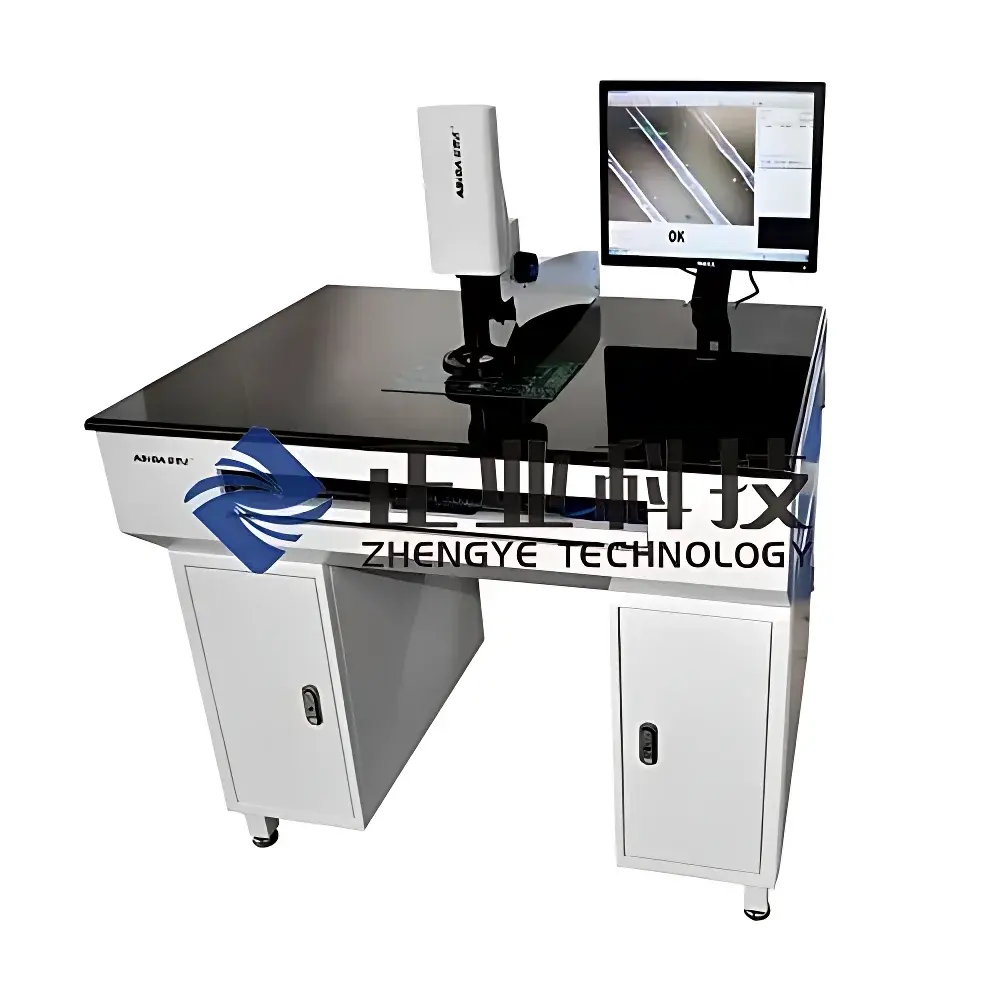
ASIDA XK23 PCB Trace Width and Spacing Measurement System
| Brand | ASIDA |
|---|---|
| Origin | Guangdong, China |
| Manufacturer Type | Authorized Distributor |
| Country of Origin | China |
| Model | XK23 |
| Pricing | Available Upon Request |
| Measurement Accuracy | ±1 µm |
| Pixel Resolution (XK23) | 0.4–2.6 µm/pixel |
| Total Magnification | 70–450× |
| Optical Zoom | 1.4–9× Continuous |
| Maximum Board Width | ≤760 mm |
| Field of View | 0.53×0.4 mm to 3.4×2.5 mm |
| Minimum Measurable Line Width | ≥20 µm |
| Instrument Dimensions (excl. PC) | 960×780×1280 mm |
| Weight | 190 kg |
Overview
The ASIDA XK23 PCB Trace Width and Spacing Measurement System is a high-precision optical metrology instrument engineered for non-contact, two-dimensional dimensional analysis of printed circuit board (PCB) and flexible printed circuit (FPC) features. It operates on the principle of digital image acquisition combined with sub-pixel edge detection algorithms, enabling quantitative measurement of trace width, spacing between conductive lines, edge-to-hole distance, circular/oval hole diameters, and arc radii. Designed for use after etching but prior to solder mask application, the system supports both inner-layer and outer-layer inspection workflows in high-mix, high-volume PCB manufacturing environments. Its modular optical architecture integrates a motorized zoom lens, high-resolution monochrome CMOS sensor, coaxial red LED illumination for rapid feature localization, and precision mechanical stage control — all calibrated to NIST-traceable standards. The system complies with IPC-TM-650 2.2.17 (Microsectioning and Image Analysis) and supports alignment with IPC-A-600 and IPC-6012 acceptance criteria for conductor geometry verification.
Key Features
- Precision optical measurement platform with continuous 1.4×–9× optical zoom and total magnification range of 70×–450×, optimized for resolution flexibility across varying trace geometries.
- Sub-pixel edge detection algorithm achieving ±1 µm measurement uncertainty (k = 2), validated per ISO/IEC 17025-compliant internal calibration protocols.
- Adjustable pixel resolution (0.4–2.6 µm/pixel at XK23 configuration), enabling optimal sampling density for features ≥20 µm without aliasing or oversampling penalties.
- Red LED coaxial illumination system for real-time visual registration and rapid operator-assisted positioning — reducing setup time by up to 40% compared to manual white-light systems.
- Integrated SPC module compliant with ASTM E2587 and ISO 7870-2, supporting real-time X̄-R charting, capability indices (Cp/Cpk), trend analysis, and automated out-of-spec alerting.
- Rigid granite-based mechanical structure with vibration-damped base and linear-motion stages, ensuring thermal and mechanical stability during extended measurement cycles.
Sample Compatibility & Compliance
The XK23 accommodates rigid PCBs up to 760 mm in width and FPC substrates with thicknesses ranging from 25 µm to 250 µm. It supports standard FR-4, polyimide, and ceramic-based laminates, as well as metal-core and high-frequency RF substrates (e.g., Rogers RO4000®). Measurement repeatability is maintained across surface finishes including ENIG, immersion silver, OSP, and HASL. All software-generated reports include audit trails meeting FDA 21 CFR Part 11 requirements for electronic records and signatures. Calibration certificates are issued per ISO/IEC 17025 by an ILAC-accredited third-party laboratory, and system validation documentation supports GLP and GMP-regulated PCB fabrication facilities.
Software & Data Management
The proprietary ASIDA MetroVision™ software provides a Windows-based interface with intuitive workflow navigation, multi-user role management (operator, engineer, QA administrator), and encrypted local database storage. Measurement data export supports CSV, XML, and PDF formats compatible with enterprise MES and QMS platforms (e.g., Siemens Opcenter, ETQ Reliance). Raw image archives are stored with embedded EXIF metadata (timestamp, magnification, lens position, calibration ID). Version-controlled firmware updates are delivered via secure HTTPS channel, with rollback capability and SHA-256 integrity verification. Software validation packages—including IQ/OQ/PQ protocols—are available upon request for regulated industries.
Applications
- Post-etch dimensional verification of fine-pitch traces (≤50 µm) in HDI and mSAP PCBs.
- Process monitoring of laser direct imaging (LDI) and photolithography tool performance through line width uniformity (LWU) trending.
- Failure analysis support for open-circuit and short-circuit root cause investigation in prototype and NPI stages.
- Qualification testing of IC substrate redistribution layers (RDL) and fan-out wafer-level packaging (FOWLP) interconnects.
- Dimensional validation of display driver flex circuits (LCD/OLED), semiconductor lead frames, and thin-film resistor patterns.
FAQ
What calibration standards does the XK23 support?
The system accepts NIST-traceable chrome-on-glass reticles (e.g., Thorlabs R1LH series) and certified step-height standards for periodic verification. Internal calibration routines cover magnification linearity, pixel pitch stability, and stage orthogonality.
Can the XK23 integrate with existing factory automation systems?
Yes — it supports Modbus TCP and OPC UA connectivity for bidirectional communication with PLCs and MES. Custom API endpoints (RESTful JSON) are available for automated job dispatch and result ingestion.
Is remote diagnostics supported?
Remote maintenance is enabled via TLS-encrypted TeamViewer QuickSupport sessions, subject to customer IT policy approval. Firmware and configuration backups can be scheduled to network-attached storage.
Does the system meet RoHS and CE directives?
Yes — the XK23 carries CE marking per EMC Directive 2014/30/EU and RoHS Directive 2011/65/EU. Declaration of Conformity and technical construction files are provided with shipment.
How is measurement uncertainty quantified and documented?
Uncertainty budgets follow GUM (JCGM 100:2008) methodology and include contributions from pixelation, lens distortion, stage repeatability, environmental drift (±0.5°C/hour), and operator variability. Full uncertainty statements accompany every exported report.


")