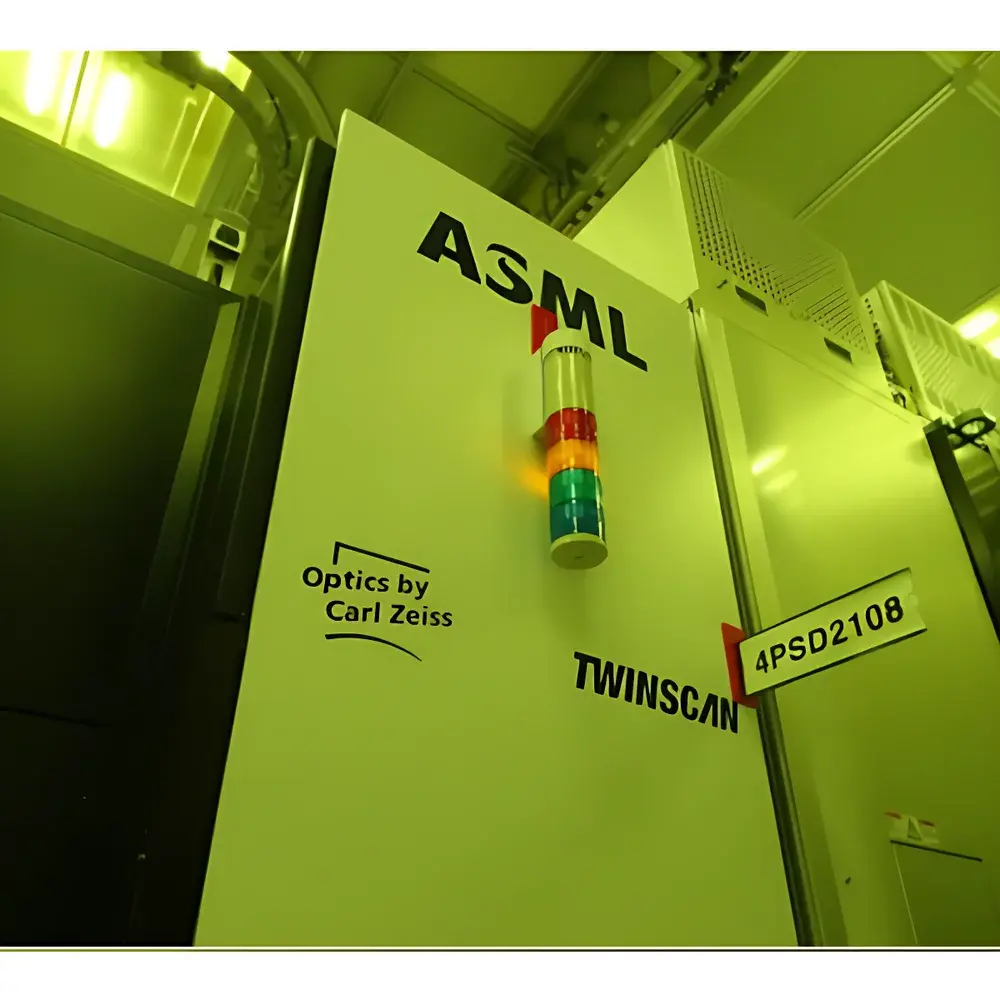
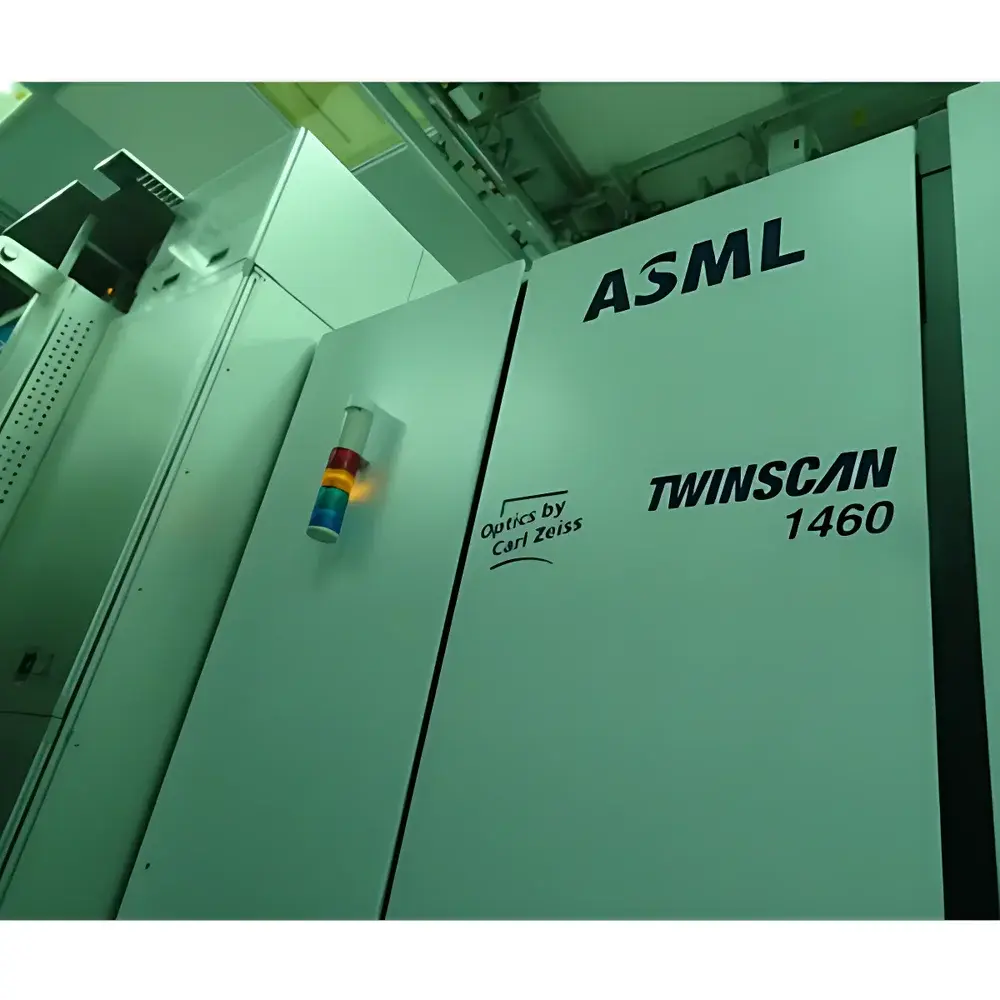

ASML 1460K Mask Aligner
| Brand | ASML |
|---|---|
| Origin | Netherlands |
| Model | 1460K |
| Type | Contact/Proximity Mask Aligner |
| Application | R&D and low-volume semiconductor prototyping, MEMS, microfluidics, academic cleanroom fabrication |
Overview
The ASML 1460K is a high-precision contact and proximity mask aligner engineered for research, development, and low-volume production environments in semiconductor laboratories, university cleanrooms, and MEMS fabrication facilities. Unlike projection lithography systems (e.g., ASML’s EUV scanners), the 1460K operates on the principle of near-field optical lithography—utilizing collimated UV light (typically at 365 nm or 405 nm) to transfer patterns from a photomask directly onto a photoresist-coated substrate. Its design emphasizes mechanical stability, sub-micron alignment accuracy, and repeatable gap control between mask and wafer—critical for achieving consistent feature resolution down to ≤2 µm in proximity mode and <1 µm in soft/hard contact mode. The system is not intended for high-throughput manufacturing but serves as a foundational tool for process development, mask qualification, rapid prototyping, and educational lithography training.
Key Features
- Motorized XYZ-theta alignment stage with digital micrometer readouts and real-time alignment verification via dual-view optical microscope (5×–50× zoom, split-field capability)
- UV illumination source with adjustable intensity (0–100%) and uniformity >95% across 150 mm wafers; compatible with standard i-line (365 nm) and h-line (405 nm) mercury lamps
- Programmable exposure timer (0.1 s–999.9 s) with automatic lamp warm-up compensation and dose calibration traceability
- Robust granite base and vibration-damped optical table integration to minimize drift during long exposures
- Interlocked safety cabinet with UV shielding, emergency stop, and door-interrupt sensing compliant with IEC 60204-1 and EN 61000-6-4 EMC standards
- Manual and semi-automated operation modes—no proprietary real-time operating system required; minimal software dependency for core functionality
Sample Compatibility & Compliance
The ASML 1460K accommodates substrates up to 150 mm (6-inch) diameter, including silicon wafers, glass slides, quartz plates, and flexible polymer films (e.g., PI, PET). It supports standard mask formats (5″ × 5″, 7″ × 7″) with frame-based mounting and vacuum chucking. Alignment fiducials are verified optically using crosshair overlays and edge-detection assist features. The system conforms to ISO 14644-1 Class 5 cleanroom compatibility when operated within controlled environments. While not certified for GMP or FDA 21 CFR Part 11 compliance out-of-the-box, its exposure logs, alignment records, and manual audit trails support GLP-aligned documentation practices when integrated into laboratory quality management systems.
Software & Data Management
The 1460K operates primarily via front-panel controls and an integrated LCD interface. Optional PC connectivity (RS-232 or USB-to-serial) enables remote exposure logging and parameter archiving via vendor-supplied ASCII-based command protocol. No embedded database or electronic signature functionality is included; all operational data—including exposure time, lamp intensity, alignment offsets, and date/time stamps—are recorded manually or exported to CSV for external LIMS or ELN integration. Audit trail generation requires procedural documentation per institutional SOPs—not automated electronic records.
Applications
- Semiconductor device prototyping: MOSFET test structures, diode arrays, thin-film transistor backplanes
- MEMS fabrication: pressure sensor diaphragms, cantilever arrays, RF resonators
- Microfluidic device patterning: PDMS master molds, SU-8 channel layers, electrode interconnects
- Optical component fabrication: diffractive optical elements (DOEs), microlens arrays, waveguide templates
- Academic instruction: hands-on lithography training, photoresist characterization, alignment methodology validation
- Mask evaluation and repair verification prior to use in stepper or scanner tools
FAQ
Is the ASML 1460K suitable for volume production?
No—it is designed for R&D, pilot-line processing, and low-yield fabrication. Its throughput, maintenance cycle, and lack of automated wafer handling preclude high-volume manufacturing use.
Does it support deep-UV (DUV) or extreme-UV (EUV) wavelengths?
No. The 1460K uses broadband mercury arc lamps with standard i-line (365 nm) and h-line (405 nm) filtering. It does not incorporate excimer lasers or reflective EUV optics.
Can it process wafers larger than 150 mm?
No. Maximum substrate size is 150 mm (6-inch); no upgrade path exists for 200 mm compatibility.
Is technical support available outside the Netherlands?
Yes—through ASML-certified service partners with regional field engineers trained in mechanical calibration, optical alignment, and lamp replacement procedures.
What photoresists are compatible with the 1460K?
Standard g-line/i-line positive resists (e.g., AZ® series, S1800, ma-N) and negative resists (e.g., SU-8, NR9) are fully supported; resist selection must match the exposure wavelength and process thermal budget.


