ASML TWINSCAN Lithography Systems – DUV, Immersion, and High-NA EUV Platforms
| Brand | ASML |
|---|---|
| Origin | Netherlands |
| Product Category | Mask Aligner / Stepper-Based Lithography System for Semiconductor Fabrication |
| Models | TWINSCAN XT:1900Gi, XT:2000i, NXT:1980Di, NXT:2050i, NXE:3400B/C, NXE:3600D, EXE:5000 Series |
| Light Source Wavelengths | 248 nm (KrF), 193 nm (ArF dry & immersion), 13.5 nm (EUV) |
| Single-Exposure Resolution | 38 nm (ArF immersion), 13 nm (EUV, NA=0.33), 8 nm (High-NA EUV, NA=0.55) |
| Throughput | Up to 275 wafers/hour (NXT:2050i), ~170 wafers/day (NXE:3400C), target 220 wafers/day (EXE:5000) |
| Supported Process Nodes | 28 nm to sub-2 nm |
| Compliance | ISO 14644-1 Class 1 cleanroom integration, SEMI S2/S8 safety standards, compatible with 300 mm wafer handling automation (SECS/GEM) |
Overview
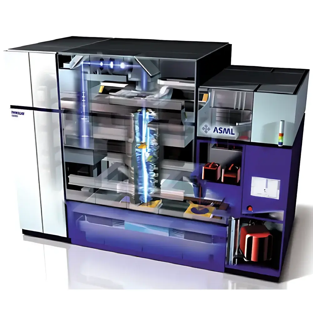
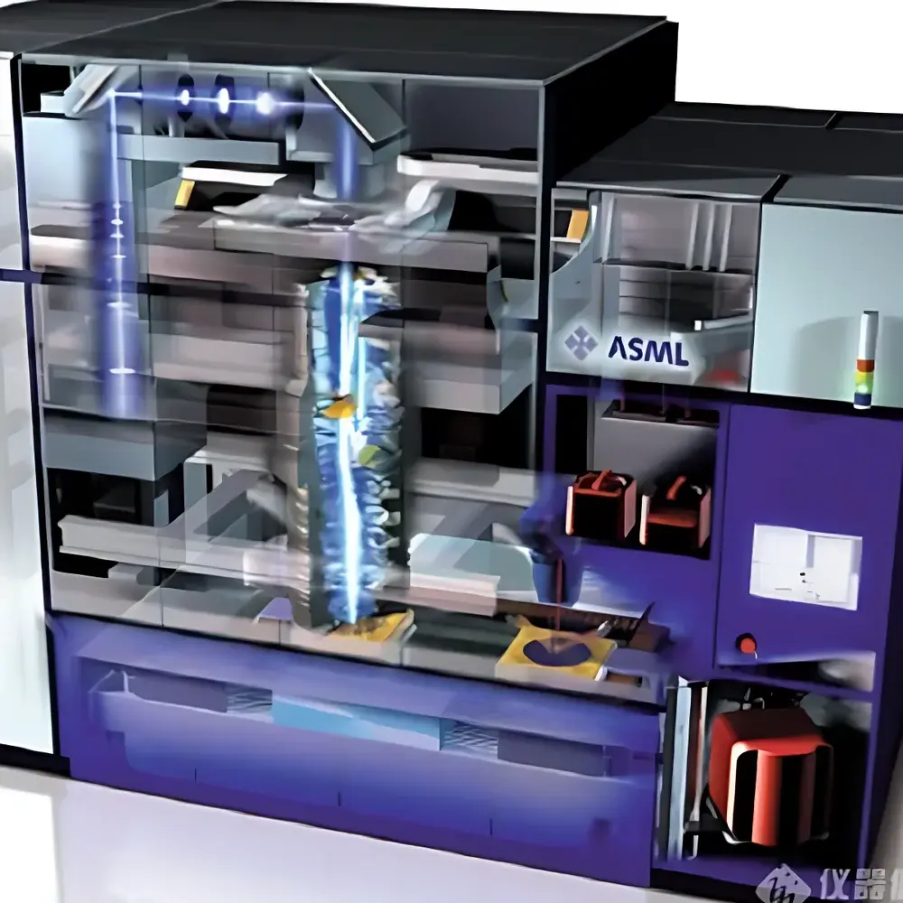
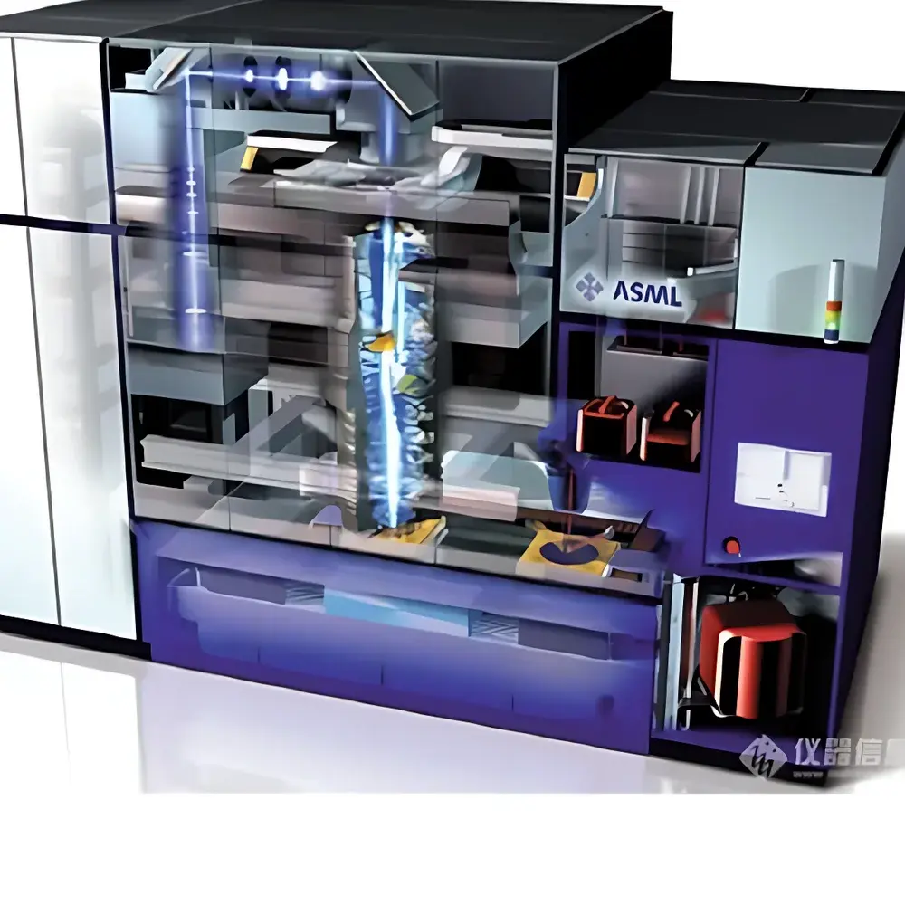
The ASML TWINSCAN lithography platform represents the industry benchmark for photolithographic patterning in semiconductor manufacturing. Engineered for precision, repeatability, and scalability across technology nodes, these systems implement three fundamental optical architectures: deep ultraviolet (DUV) dry and immersion projection lithography, extreme ultraviolet (EUV) lithography at 13.5 nm, and next-generation high-numerical-aperture (High-NA) EUV systems. Each architecture is built upon ASML’s proprietary scanner architecture—featuring synchronized wafer and reticle stages, adaptive illumination optics, and real-time aberration correction—to ensure nanometer-level overlay control (< 1.5 nm 3σ) and critical dimension uniformity (CDU < 1.0 nm). Unlike mask aligners used in MEMS or packaging, TWINSCAN systems are step-and-scan projection tools designed for high-volume manufacturing (HVM) of logic, memory, and foundry devices on 300 mm silicon wafers.
Key Features
- Modular Scanner Architecture: Dual-stage motion control enables continuous scanning during exposure while the second stage pre-aligns the next die—maximizing duty cycle and throughput.
- Adaptive Illumination: Programmable illuminator (e.g., FlexRay™) supports off-axis, dipole, quadrupole, and custom source-mask optimization (SMO) for enhanced process window and resolution.
- Real-Time Metrology Integration: On-board interferometric alignment sensors, focus mapping, and dose control ensure sub-nanometer overlay stability and CD consistency across full-wafer fields.
- Immersion Fluid Management: Precision fluid confinement system for ArF immersion platforms maintains stable water layer thickness (< ±0.5 nm variation) between lens and resist surface—critical for maintaining λ/NA resolution scaling.
- EUV Source & Collector Optimization: LPP (laser-produced plasma) source with debris mitigation and multilayer Mo/Si collector mirrors deliver stable 13.5 nm radiation with >250 W power at intermediate focus (IF) for NXE:3400C and beyond.
- High-NA Optics: EXE:5000 series integrates an innovative 0.55 NA reflective objective with a six-mirror design, enabling single-exposure patterning down to 8 nm half-pitch and reducing multi-patterning complexity for sub-3 nm logic nodes.
Sample Compatibility & Compliance
TWINSCAN systems are engineered for 300 mm silicon wafers with standard edge exclusion (≤ 3 mm) and backside flatness compliance per SEMI MW202. Reticle compatibility includes 6-inch quartz masks with chromium or attenuated phase-shift layers, supported by automated reticle exchange and particle-free handling. All platforms meet ISO 14644-1 Class 1 cleanroom interface requirements and integrate seamlessly with factory automation via SECS/GEM and GEM300 protocols. For regulated environments, ASML provides audit-ready documentation packages supporting FDA 21 CFR Part 11 (electronic records/signatures), ISO 9001 quality management, and IEC 61508 functional safety certification for critical motion and interlock subsystems. The systems are routinely deployed in GMP-compliant fabs producing automotive-grade ICs (AEC-Q100 qualified processes) and medical ASICs requiring full traceability and change control.
Software & Data Management
LithoTrack™ software suite provides unified control across DUV, EUV, and High-NA platforms—including recipe management, exposure logging, fault diagnostics, and predictive maintenance analytics. All exposure parameters (dose, focus, overlay offsets, illumination settings) are logged with timestamped metadata compliant with ASTM E1578-22 (standard guide for semiconductor equipment data formats). Integrated with fab-wide MES and APC systems, LithoTrack supports closed-loop process control using run-to-run (R2R) and advanced process control (APC) algorithms. Audit trails record all operator actions, parameter changes, and calibration events—fully traceable for GLP/GMP audits. Remote monitoring and secure firmware updates are delivered via ASML’s certified TLS 1.3–secured service portal, with optional air-gapped deployment for export-controlled facilities.
Applications
- High-volume production of logic ICs (mobile SoCs, AI accelerators) at 7 nm, 5 nm, 3 nm, and sub-2 nm nodes using NXE and EXE platforms.
- Mature-node manufacturing (28 nm to 90 nm) for power management ICs, analog/mixed-signal chips, and automotive microcontrollers—optimized on XT and NXT DUV platforms.
- Advanced packaging applications including fan-out wafer-level packaging (FOWLP), 2.5D/3D interposers, and chiplet integration—supported by i-line systems such as XT:860N.
- MEMS, RF filters, and compound semiconductor device fabrication requiring large-field, high-throughput patterning with i-line or KrF sources.
- Research and development of novel resists, underlayers, and etch stacks—leveraging flexible illumination modes and dose/focus matrix capabilities.
FAQ
What distinguishes DUV immersion from EUV lithography in terms of process capability?
DUV immersion (193i) achieves ~38 nm resolution via water immersion and multiple patterning; EUV (13.5 nm) enables single-exposure patterning below 13 nm, eliminating complex multi-patterning but requiring vacuum operation and specialized photoresists.
Is the EXE:5000 platform compatible with existing fab infrastructure?
The EXE:5000 requires upgraded cleanroom vibration isolation (≤ 50 nG RMS), enhanced thermal stability (±0.01 °C ambient control), and higher electrical capacity (≥ 2.5 MVA); retrofitting is feasible but demands comprehensive facility assessment.
How does ASML support regulatory compliance for medical or automotive IC manufacturing?
ASML delivers full validation documentation packages (IQ/OQ/PQ), change control logs, and 21 CFR Part 11–compliant electronic signature workflows—validated in collaboration with leading IDMs and foundries operating under IATF 16949 and ISO 13485 frameworks.
Can TWINSCAN systems be integrated into a fully automated smart fab?
Yes—all models support SEMI E30 (GEM), E40 (Equipment Communications Standard), and E148 (Process Data Collection) standards, enabling bidirectional communication with MES, APC, and digital twin platforms.
What is the typical lead time and service support model for NXE-series tools?
Lead times exceed 18 months due to supply chain constraints; ASML provides 24/7 remote diagnostics, on-site field engineers, and spare-part logistics aligned with SLAs covering >95% uptime for HVM deployments.


