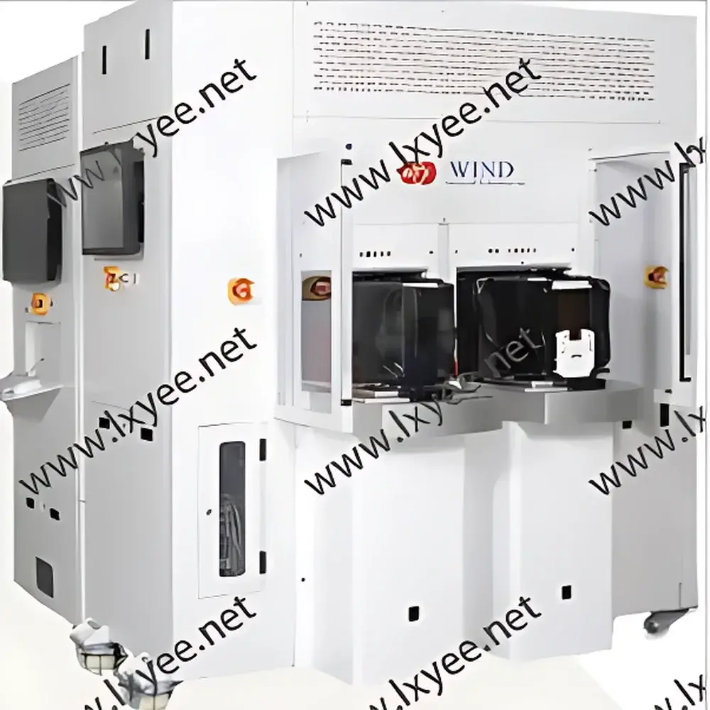


ATI WIND Wafer Inspection System
| Brand | ATI |
|---|---|
| Model | WIND |
| Category | Wafer Defect Electron Beam Inspection Equipment |
| Origin | South Korea |
| Frame Material | Hairline Stainless Steel with White Powder Coating |
| Dimensions (W×D×H) | 1900 mm × 1680 mm × 2100 mm |
| Weight | 3.5 tons |
| Wafer Compatibility | 200 mm & 300 mm bare wafers |
| Load Port Support | FOUP, open cassette, ring cassettes (8″, 12″) |
| Alignment | Dual-wafer-size auto-alignment (200/300 mm bare |
| Automation Interface | SECS/GEM compliant, SEMI E84 standard |
| Vision System | Dual-optic 2D/3D module with real-time auto-focus |
| Inspection Modes | Normal/sawing inspection, bump inspection, edge/kerf measurement, 3D bump height/warpage/coplanarity/thickness/BLT metrology |
| Algorithm | Die-to-Die (D2D) registration using optimal die selection from adjacent four dies |
| Optional Module | IR imaging for subsurface crack and silicon bulk defect detection |
| Compliance | Fully aligned with SEMI standards |
Overview
The ATI WIND Wafer Inspection System is a high-precision, dual-mode optical inspection platform engineered for front-end and back-end semiconductor manufacturing environments. Unlike conventional optical or electron-beam systems constrained to single-mode operation, the WIND integrates synchronized 2D and 3D optical metrology within a unified mechanical architecture—enabling simultaneous defect classification and quantitative topographic measurement on both bare and ring-framed wafers. Its core inspection principle relies on structured illumination combined with high-resolution telecentric optics and real-time z-axis auto-focus control, delivering sub-micron lateral resolution and nanometer-level vertical repeatability in production-grade throughput. Designed specifically for post-thinning, post-dicing, and post-bonding process verification, the WIND addresses critical yield loss vectors including micro-cracks, NCF voids, probe mark anomalies, bump coplanarity deviations, and kerf geometry inconsistencies—without requiring vacuum chambers or conductive coating.
Key Features
- Dual-optic modular vision system: Independent 2D high-speed imaging path and 3D confocal profilometry path, both calibrated to a common coordinate frame for traceable metrology.
- Real-time auto-focus engine: Closed-loop piezoelectric Z-stage with feedback from integrated focus sensors ensures consistent focus across full wafer maps—even over warped or翘曲 substrates up to 150 µm TTV.
- Flexible substrate handling: Native support for 200 mm and 300 mm bare wafers, plus automatic recognition and alignment of 300 mm and 400 mm ring-framed carriers—enabling seamless transition between wafer formats without mechanical reconfiguration.
- SEMI-compliant automation stack: Full SECS/GEM implementation (300 mm class), SEMI E84 certified communication protocol, and hardware-level handshake signaling for integration into factory-wide MES and AMHS infrastructures.
- Proprietary D2D registration algorithm: Selects optimal reference die from adjacent four-die cluster to minimize pattern distortion impact—critical for advanced packaging nodes where overlay error < 50 nm is required.
- IR inspection option: Integrated near-infrared (NIR) illumination at 1310 nm wavelength enables non-destructive subsurface imaging for detecting cleavage cracks, silicon bulk fractures, and delamination beneath passivation layers.
Sample Compatibility & Compliance
The WIND accommodates industry-standard carrier types including FOUPs (Front Opening Unified Pod), open cassettes, and ring cassettes (8″ and 12″). Its mechanical frame—constructed from hairline-finished stainless steel with electrostatic-dissipative white powder coating—meets ISO Class 5 cleanroom compatibility requirements. All motion subsystems are rated for continuous 24/7 operation under Class 100 particle conditions. From a regulatory standpoint, the system’s data acquisition firmware supports audit-trail generation per FDA 21 CFR Part 11, including electronic signature capture, user access control tiers, and immutable log archiving. It conforms to SEMI S2/S8 safety guidelines and includes built-in validation modules for periodic performance verification (e.g., NIST-traceable step-height standards, particle size calibration targets).
Software & Data Management
The WIND operates under ATI’s proprietary INSIGHT™ software suite—a modular, Windows-based platform supporting both recipe-driven automated inspection and interactive metrology analysis. The software features embedded statistical process control (SPC) dashboards compliant with MSA AIAG guidelines, configurable defect binning logic based on ASTM F2121 classification rules, and direct export to JMP, MATLAB, and Yield Ramp databases via ODBC and OPC UA interfaces. Raw image and height-map datasets are stored in vendor-neutral HDF5 format with embedded metadata (timestamp, tool ID, operator ID, environmental logs). Version-controlled recipe management ensures GMP-aligned change control, while encrypted local storage and TLS 1.3–secured remote diagnostics uphold cybersecurity best practices outlined in NIST SP 800-53 Rev. 5.
Applications
The WIND serves as a primary inline inspection solution for advanced packaging processes—including fan-out wafer-level packaging (FOWLP), 2.5D/3D IC stacking, and hybrid bonding lines. Typical use cases include: post-saw inspection of dicing streets for chipping and micro-crack propagation; post-grinding thickness uniformity mapping; bump height and coplanarity screening prior to flip-chip assembly; warpage quantification after temporary bond/debond cycles; and BLT (backside lithography thickness) verification following thinning. Its ability to perform simultaneous 2D defect detection and 3D metrology eliminates the need for separate tools—reducing floor space, cross-tool calibration drift, and total cost of ownership in high-mix, low-volume advanced packaging fabs.
FAQ
Does the WIND support both optical and electron-beam inspection modes?
No—the WIND is an optical inspection system utilizing visible and near-infrared wavelengths. It does not incorporate electron-beam optics; its high-resolution capability derives from proprietary telecentric lens design and confocal depth discrimination.
Can the system inspect wafers with temporary bonding films?
Yes—its real-time auto-focus and multi-wavelength illumination enable stable imaging through polymer-based temporary adhesives (e.g., DVS, Revalpha) and glass carriers up to 1 mm thick.
Is the 3D measurement traceable to national standards?
Yes—height measurements are calibrated using NIST-traceable step-height standards (e.g., VLSI Standards SRM 2100 series), with documented uncertainty budgets provided in the system’s Certificate of Calibration.
What level of integration is supported with factory automation systems?
Full SECS/GEM v5.0 and SEMI E84 compliance ensures plug-and-play integration with major MES platforms (e.g., Applied Materials EnduraLink, Tokyo Electron TELiS), including lot start/stop messaging, alarm forwarding, and remote recipe push.
How is system performance validated over time?
The WIND includes an on-board validation module with automated daily self-check routines—covering focus stability, illumination uniformity, stage positioning accuracy, and defect detection sensitivity—generating PDF reports compliant with ISO/IEC 17025 internal audit requirements.


