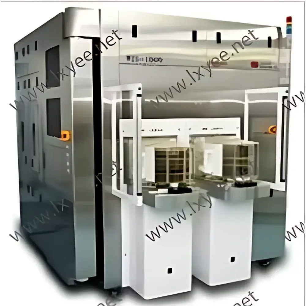
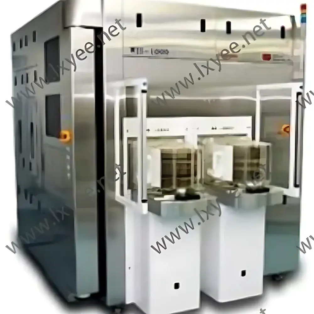
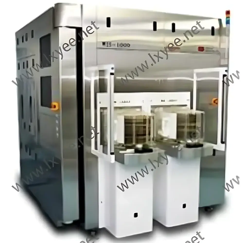
ATI WIS-1000 Wafer Inspection System
| Brand | ATI |
|---|---|
| Origin | Germany |
| Manufacturer Type | Authorized Distributor |
| Product Category | Imported Instrument |
| Model | WIS-1000 |
| Instrument Type | Optical Patterned Wafer Defect Inspection System |
| Target Applications | Semiconductor Front-End Process Monitoring |
| Process Node Support | Sub-28 nm FinFET and FD-SOI Technologies |
| Compatible Wafer Sizes | 200 mm and 300 mm |
| Throughput | Up to 120 wafers per hour (depending on inspection recipe and defect density) |
| Optical Resolution | ≤ 150 nm (at λ = 405 nm, high-NA dark-field imaging) |
| Defect Detection Sensitivity | ≥ 95% for ≥ 80 nm particles and ≥ 120 nm pattern bridging/bridging defects on metal and dielectric layers |
| Compliance | ISO 9001-certified manufacturing |
Overview
The ATI WIS-1000 Wafer Inspection System is a high-performance, automated optical inspection platform engineered for in-line detection of surface and patterned defects on semiconductor wafers during front-end-of-line (FEOL) and middle-of-line (MOL) fabrication. Utilizing advanced dark-field illumination combined with high-numerical-aperture (NA) optics and multi-spectral imaging, the WIS-1000 identifies sub-150 nm physical anomalies—including particles, scratches, pattern bridging, missing features, and micro-scratches—on bare silicon, oxide, nitride, and metallized wafers. Designed for integration into 300 mm fab environments, the system supports both manual and fully automated load-port configurations, enabling seamless interface with standard FOUPs and SMIF pods. Its modular architecture allows for field-upgradable illumination modes (e.g., broadband LED, UV-enhanced, and polarized variants), ensuring adaptability across evolving process requirements—from mature nodes to advanced logic and memory technologies.
Key Features
- High-sensitivity dark-field optical engine optimized for sub-28 nm node defect capture on patterned wafers
- Dual-wavelength imaging capability (405 nm + 635 nm) for enhanced contrast differentiation between topography-induced and material-based scattering events
- Real-time autofocus and auto-alignment algorithms compensating for wafer warp, thickness variation, and chuck tilt
- Integrated stage motion control with ≤ ±0.5 µm positioning repeatability over full 300 mm travel range
- Configurable inspection recipes supporting die-to-die (D2D), die-to-database (D2DB), and hybrid comparison modes
- Robust thermal management system maintaining optical path stability within ±0.1 °C over 8-hour continuous operation
Sample Compatibility & Compliance
The WIS-1000 accommodates standard 200 mm and 300 mm silicon wafers, including those with low-k dielectrics, copper interconnects, and high-aspect-ratio etch structures. It is qualified for use in Class 100 cleanroom environments and conforms to SEMI E10 (Specification for Definition and Measurement of Equipment Reliability, Maintainability, and Availability), SEMI E11 (Equipment Communication Standard), SEMI E120 (SECS/GEM Interface Standard), and SEMI E142 (Data Collection and Reporting Standard). The system supports audit-ready logging compliant with ISO 9001 quality management protocols and provides traceable calibration records aligned with NIST-traceable reference standards.
Software & Data Management
The proprietary ATI VisionInsight™ software suite delivers intuitive recipe creation, real-time defect classification using supervised machine learning models (trained on >500K labeled defect images), and hierarchical binning by morphology, location, and process layer. All inspection data—including raw images, coordinate maps, and classification confidence scores—is stored in an encrypted SQLite database with optional integration into factory-wide MES via SECS/GEM or OPC UA interfaces. Audit trails meet GLP/GMP requirements, including user authentication, change history, and electronic signature support per FDA 21 CFR Part 11 guidelines.
Applications
- Post-lithography defect screening for reticle-induced printing errors and resist scumming
- In-process monitoring after CMP to detect residual slurry particles and dishing-related anomalies
- Pre-etch verification of mask integrity and pattern fidelity on hardmask layers
- Final wafer acceptance testing prior to shipment to backend assembly partners
- Root-cause analysis support through correlation with inline metrology tools (e.g., CD-SEM, OCD)
FAQ
What wafer sizes does the WIS-1000 support?
The system supports both 200 mm and 300 mm diameter wafers, with automatic size recognition and stage reconfiguration.
Is the WIS-1000 compatible with existing fab automation infrastructure?
Yes—it complies with SEMI E120 and E142 standards and integrates natively with major MES platforms via SECS/GEM or OPC UA protocols.
Does the system provide quantitative defect classification?
Yes—VisionInsight™ includes trained classifiers for 12+ defect types (e.g., particle, bridge, open, notch) with configurable sensitivity thresholds and false-positive suppression filters.
Can inspection recipes be transferred between WIS-1000 units?
Yes—recipes are portable across identical configurations and include embedded calibration metadata for cross-system reproducibility.
What maintenance intervals are recommended for optical subsystems?
Lens cleaning and illumination uniformity validation are scheduled every 250 operating hours; full optical recalibration is recommended annually or after any mechanical shock event.


