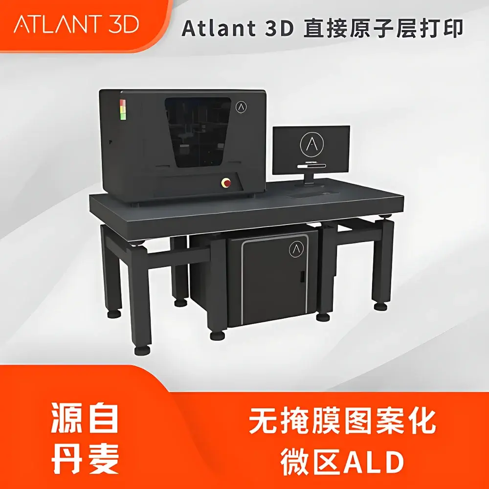
Atlant 3D NANOFABRICATOR™ LITE Direct Atomic Layer Fabrication System
| Brand | ATLANT3D |
|---|---|
| Origin | Denmark |
| Manufacturer Type | Authorized Distributor |
| Product Origin | Imported |
| Model | NANOFABRICATOR™ LITE |
| Substrate Size | Up to 4-inch wafers |
| Process Temperature Range | 50 °C – 300 °C |
| Precursor Channels | 2 |
| Dimensions (W × H × D) | 1400 mm × 800 mm × (depth not specified) |
| Thickness Uniformity | Capable of controlled thickness gradients across substrate |
Overview
The Atlant 3D NANOFABRICATOR™ LITE is a benchtop-scale direct atomic layer fabrication system engineered for spatially selective, atmospheric-pressure atomic layer processing (ALP). Unlike conventional atomic layer deposition (ALD) tools requiring high-vacuum chambers and photolithographic patterning, this platform implements Direct Atomic Layer Processing (DALP®)—a patented spatial ALD methodology that decouples precursor delivery via micro-nozzle arrays. Chemical precursors are delivered in parallel but physically separated streams to predefined substrate locations, enabling surface-confined reactions without global exposure. This eliminates the need for masks, etch steps, or vacuum pumping cycles, reducing process complexity while preserving atomic-scale thickness control and sub-micrometer lateral resolution. The system operates at ambient pressure, significantly lowering infrastructure demands and enabling integration into standard cleanroom or lab environments without dedicated vacuum utilities.
Key Features
- Maskless, direct-write atomic layer fabrication: Enables real-time pattern definition without photomasks, lithography, or post-deposition etching.
- Dual-precursor architecture: Supports sequential or co-injected delivery of two chemically distinct precursors—optimized for binary metal oxides, nitrides, sulfides, and functionalized surfaces.
- Atmospheric-pressure operation: Eliminates vacuum pumps, load locks, and associated maintenance; reduces power consumption by >70% versus conventional ALD systems.
- Gradient-enabled deposition: Programmable nozzle translation and pulse timing allow continuous thickness modulation across substrates—e.g., linear, radial, or user-defined gradient profiles up to 10 mm total thickness range.
- Integrated metrology-ready interface: Compatible with in situ optical reflectometry and ex situ SEM/EDX for rapid process validation and cross-sectional analysis.
- Sub-micrometer positional accuracy: Achieves ~1 µm alignment tolerance using on-substrate fiducial marker deposition and integrated camera-based registration.
Sample Compatibility & Compliance
The NANOFABRICATOR™ LITE accommodates substrates up to 4 inches (100 mm) in diameter, including silicon wafers, fused silica, sapphire, alumina, black silicon, anodized aluminum oxide (AAO), and flexible polymer foils. It demonstrates conformal coating on high-aspect-ratio structures (≥60 µm depth, 90° sidewalls) and rough surfaces (Ra ≤25 µm). All hardware and software components comply with CE marking requirements for electromagnetic compatibility (EMC Directive 2014/30/EU) and low-voltage safety (LVD Directive 2014/35/EU). Process workflows support GLP-compliant documentation when paired with optional audit-trail logging modules. While not certified to ISO 13485 or FDA 21 CFR Part 11 out-of-the-box, the system’s deterministic, script-driven operation enables full traceability of recipe parameters, timestamps, and actuator commands—facilitating internal validation for regulated R&D environments.
Software & Data Management
The system runs on Atlant 3D’s proprietary DALP Studio™ software suite, built on a modular Python-based framework with native support for GDS-II and DXF file import. Users define geometries via vector editing or CAD integration, then simulate deposition outcomes using physics-informed models calibrated against empirical growth rates. Real-time feedback from integrated pressure sensors and thermal monitoring enables closed-loop adjustments during run execution. All process data—including nozzle position, pulse duration, temperature logs, and gas flow traces—are stored in HDF5 format with timestamped metadata. Export options include CSV, TIFF (for thickness maps), and JSON for integration with LIMS or MES platforms. Optional AI-assisted mode leverages supervised learning models trained on historical growth datasets to recommend optimal parameter sets for new material combinations or geometry constraints.
Applications
- Semiconductor prototyping: Rapid development of gate-all-around (GAA) transistor dielectrics, FinFET interfacial passivation layers, and 3D IC through-silicon via (TSV) liners—bypassing mask fabrication delays and etch-induced damage.
- Photonic integrated circuits (PICs): Localized deposition of tunable refractive index layers (e.g., TiO2/SiO2 stacks) directly onto waveguide facets or resonator sidewalls.
- Quantum device fabrication: Site-specific growth of superconducting NbN or Al films on qubit test structures, with thickness gradients used to map critical current vs. film morphology.
- MEMS and sensor engineering: Conformal electrode coating (e.g., Pt on microcantilevers), functionalized sensing layers (e.g., TiO2 gradients for gas-selective response), and microfluidic channel surface modification.
- Advanced materials research: Combinatorial screening of multi-material interfaces, graded heterostructures for thermoelectrics, and defect-engineered oxide semiconductors.
FAQ
How does DALP® differ from conventional spatial ALD?
DALP® uses dynamically positioned micro-nozzles to deliver precursors with micron-level spatial fidelity, whereas traditional spatial ALD relies on fixed showerhead nozzles and substrate translation—limiting resolution and gradient flexibility.
Can the NANOFABRICATOR™ LITE perform atomic layer etching (ALE)?
Yes—by alternating oxidizing and reducing precursors in sequence, the system supports selective ALE modes for controlled material removal with sub-nanometer per-cycle precision.
Is vacuum required for any operational mode?
No. All deposition, etching, and surface modification processes occur at ambient pressure and room-temperature inert gas environment (N2 or Ar).
What materials have been successfully processed on this platform?
Validated chemistries include Al2O3, TiO2, HfO2, ZnO, Pt, Ru, SiO2, and TaN—using standard metalorganic and halide precursors compatible with low-temperature ALD.
Does the system support automated recipe transfer between instruments?
Yes. Recipes are saved as portable XML files containing all geometric, temporal, and gas-flow parameters—enabling reproducible scaling from NANOFABRICATOR™ LITE to production-grade DALP® tools.


