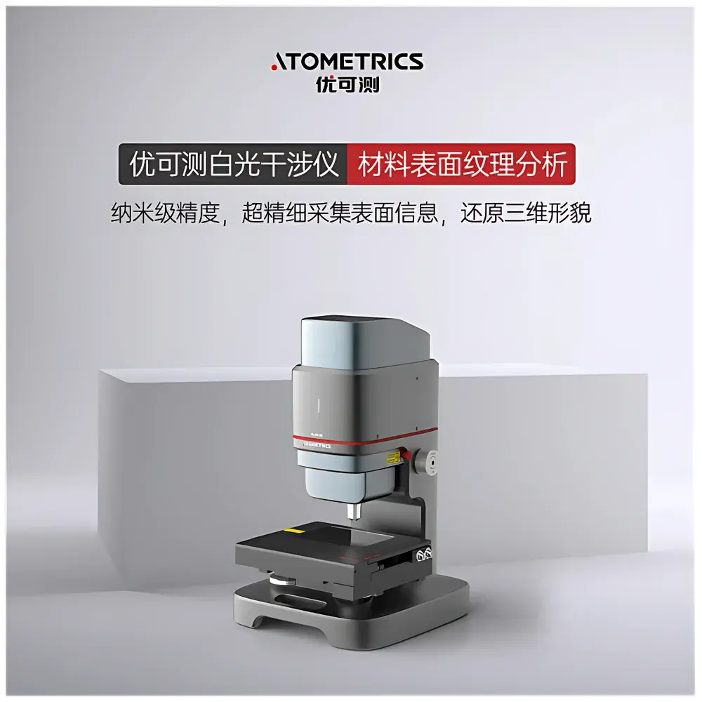
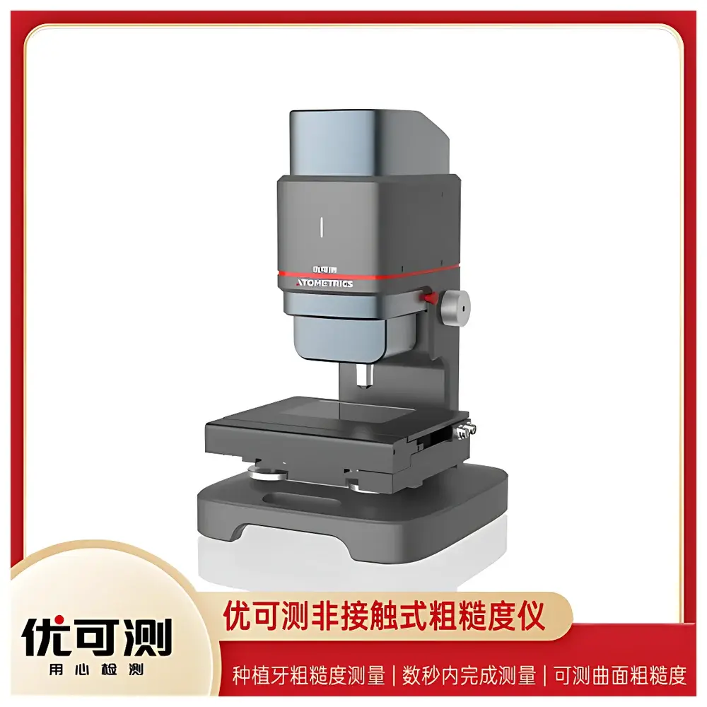
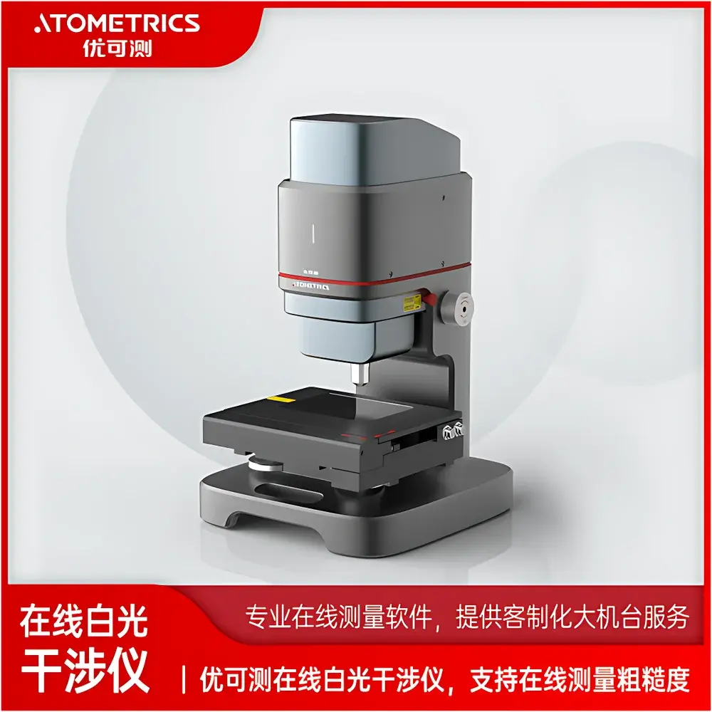
Atometrics AM-7000 Series NA-500 White-Light Interferometric Profilometer
| Brand | Atometrics |
|---|---|
| Origin | Guangdong, China |
| Manufacturer Type | OEM Manufacturer |
| Product Category | Domestic |
| Model | NA-500 |
| Pricing | Upon Request |
| Instrument Type | Non-contact Profilometer / Surface Roughness Analyzer |
| Operating Principle | White-Light Interferometry |
| Vertical Resolution | Sub-nanometer (≤ 0.03 nm) |
| Scan Speed | Up to 400 µm/s |
| Measurement Range | Large-Range Vertical Scanning (Typical Z-range > 10 mm) |
| Compliance | ISO 25178-2, ISO 4287, ASTM E1392, USP <1058> (for instrument qualification) |
Overview
The Atometrics AM-7000 Series NA-500 is a high-precision, non-contact white-light interferometric profilometer engineered for quantitative 3D surface topography analysis at sub-nanometer vertical resolution. Based on the principle of spectral-domain white-light interferometry, the system captures interference fringes generated by the superposition of reference and object beams across a broadband visible spectrum. By precisely locating the envelope maximum of the interference signal—via fast Fourier transform (FFT) or centroid-based algorithms—the NA-500 determines absolute surface height with exceptional repeatability and minimal measurement uncertainty. Its opto-mechanical architecture integrates a high-stability Michelson-type interferometer, a high-numerical-aperture (NA) objective lens turret (including 5×–100× magnifications), and a large-range piezoelectric scanner capable of vertical displacements exceeding 10 mm. This configuration enables robust characterization of both ultra-smooth optics (e.g., laser mirrors, EUV substrates) and high-aspect-ratio microstructures (e.g., MEMS trenches, etched vias, wafer bump profiles) without probe wear or surface deformation.
Key Features
- Sub-nanometer vertical resolution (≤ 0.03 nm RMS) validated per ISO 25178-6 calibration protocols
- High-speed vertical scanning up to 400 µm/s, enabling rapid acquisition of full-field 3D topography maps (up to 2048 × 2048 pixels)
- Modular objective lens system supporting magnifications from 5× to 100×, optimized for varying lateral resolution requirements (down to ~0.3 µm)
- Automated focus search and real-time fringe contrast optimization for consistent measurement fidelity across heterogeneous surfaces
- Ruggedized mechanical design with active vibration isolation compatibility and thermal drift compensation (±0.05 nm/°C typical)
- Integrated motorized X-Y stage (100 mm × 100 mm travel, 0.1 µm repeatability) for automated stitching of multi-field measurements
Sample Compatibility & Compliance
The NA-500 accommodates samples ranging from 10 mm × 10 mm wafers to 300 mm full-diameter semiconductor substrates, as well as irregularly shaped components in aerospace and precision machining applications. It supports transparent, reflective, semi-transparent, and highly scattering surfaces—including silicon, sapphire, fused silica, polished metals, thin-film stacks, and polymer coatings—without requiring conductive coating or vacuum environments. All measurement algorithms and calibration routines comply with international standards for surface texture metrology: ISO 25178-2 (areal surface texture parameters), ISO 4287 (profile-based roughness), ASTM E1392 (interferometric profilometer verification), and USP guidelines for analytical instrument qualification (AIQ). The system supports GLP/GMP-compliant audit trails and user-access controls aligned with FDA 21 CFR Part 11 requirements when configured with optional software modules.
Software & Data Management
The NA-500 operates with Atometrics’ proprietary SurfaceView™ v5.2 software platform, a Windows-based application built on .NET Framework with native support for 64-bit processing and multi-threaded data acquisition. SurfaceView provides comprehensive analysis tools including ISO 25178-defined parameters (Sa, Sq, Sz, Sdr, Vmp), cross-sectional profiling, step-height quantification (with edge-detection accuracy ≤ 2 nm), curvature mapping, and defect detection via height thresholding and gradient analysis. Raw interferogram data is stored in vendor-neutral HDF5 format; processed results export to CSV, STEP AP214, and Metrology XML (MXL) for traceable reporting. Software includes integrated instrument qualification workflows (IQ/OQ/PQ), electronic signature capability, and configurable report templates meeting internal QA and external regulatory submission requirements.
Applications
- Semiconductor manufacturing: Critical dimension verification of CMP planarization, trench depth uniformity, and photomask defect metrology
- Optics & photonics: Surface flatness assessment of laser cavity mirrors, anti-reflective coating uniformity, and diffractive optical element (DOE) profile fidelity
- Advanced packaging: Cu pillar height variation, under-bump metallization (UBM) topography, and solder joint coplanarity analysis
- Aerospace turbine components: Thermal barrier coating roughness, blade leading-edge radius validation, and EDM recast layer characterization
- Biomedical devices: Microfluidic channel depth consistency, stent strut surface finish, and implant-grade titanium roughness profiling per ISO 10993-22
- Materials R&D: In-situ wear track evolution, thin-film delamination quantification, and nanocomposite dispersion homogeneity mapping
FAQ
What is the maximum measurable step height without phase ambiguity?
The NA-500 achieves unambiguous step height measurement up to ±5 mm using its large-range piezo scanner and coherence-gated fringe analysis—no synthetic wavelength or multi-wavelength fusion required.
Can the system measure transparent thin films on silicon substrates?
Yes. The white-light source’s short coherence length enables precise interface localization at both air/film and film/substrate boundaries, allowing independent thickness and surface topography reconstruction.
Is environmental temperature control mandatory for sub-nanometer repeatability?
While not strictly mandatory, operation within a stabilized lab environment (20 ± 1°C, <40% RH) is recommended to maintain specified vertical repeatability; built-in thermal drift compensation mitigates but does not eliminate ambient effects.
Does the system support automated pass/fail inspection against GD&T tolerances?
Yes—SurfaceView™ supports custom tolerance zones, geometric feature extraction (planes, cylinders, spheres), and statistical process control (SPC) charting directly linked to CAD nominal models.
What calibration standards are supplied with the NA-500?
Each unit ships with NIST-traceable step-height artifacts (100 nm, 1 µm, 5 µm SiO₂-on-Si standards) and a certified roughness reference sample (Ra = 0.05 µm, Sa = 0.07 µm) compliant with ISO 5436-1.