Atometrics AF-T050 Spectral Reflectometry Thin-Film Thickness Metrology System
| Brand | Atometrics |
|---|---|
| Origin | Guangdong, China |
| Manufacturer Type | OEM/ODM Manufacturer |
| Regional Category | Domestic (China) |
| Model | AF-T050 |
| Pricing | Available Upon Request |
Overview
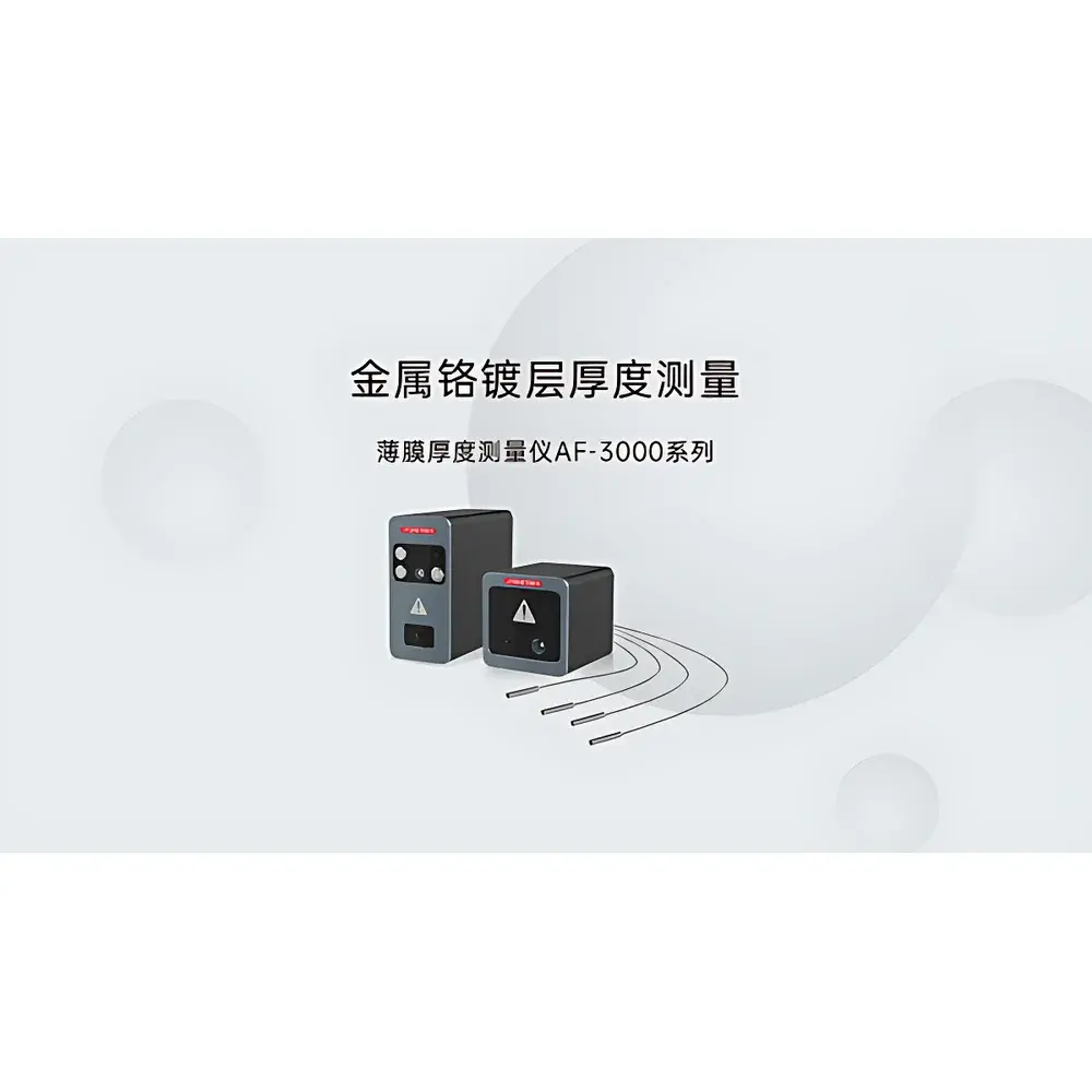
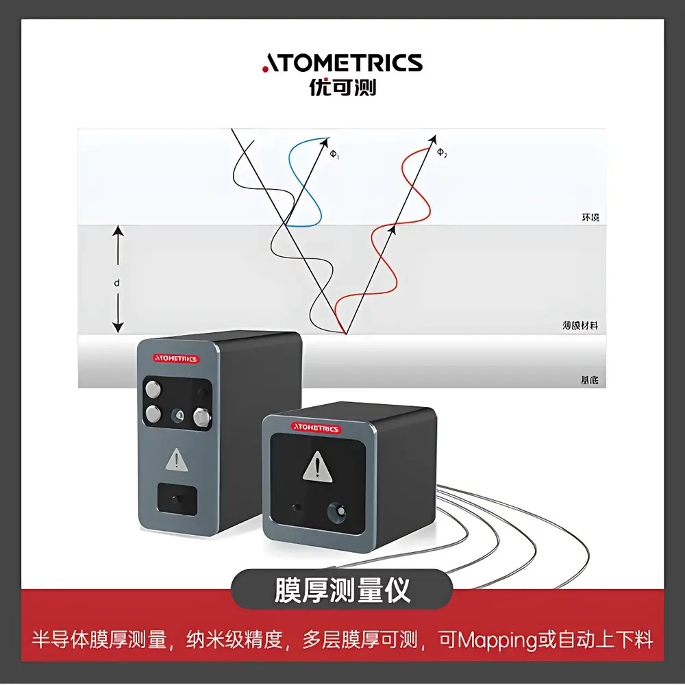
The Atometrics AF-T050 is a high-precision spectral reflectometry-based thin-film thickness metrology system engineered for non-contact, non-destructive measurement of single- and multi-layer thin films on rigid and flexible substrates. It operates on the physical principle of optical interference: incident broadband light reflects at each interface within a layered structure, generating wavelength-dependent constructive and destructive interference patterns. By acquiring high-resolution reflectance spectra across the deep ultraviolet to near-infrared range (180–2400 nm), the AF-T050 reconstructs film thicknesses and optical constants (n, k) through rigorous inverse modeling using proprietary segmented spectral fitting algorithms. Unlike conventional broad-band fitting approaches that assume uniform dispersion models across the entire spectrum, the AF-T050 implements a segmented fitting architecture—dividing the spectrum into physically meaningful sub-bands (e.g., UV, visible, NIR) and applying optimized optical dispersion models per segment. This methodology significantly reduces systematic fitting residuals, enabling sub-angstrom (≤0.1 nm) thickness resolution for ultra-thin films such as ITO (<20 nm), perovskite absorbers, and quantum dot monolayers.
Key Features
- Multi-source illumination: Deuterium lamp (180–370 nm) + tungsten-halogen lamp (320–2400 nm), ensuring continuous, spectrally stable coverage without gaps or intensity discontinuities
- Segmented spectral fitting engine: Dynamically partitions the measured reflectance spectrum into physically coherent bands and applies layer-specific dispersion models (e.g., Tauc-Lorentz, Cody-Lorentz) to minimize fitting error propagation
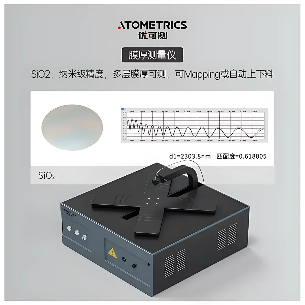
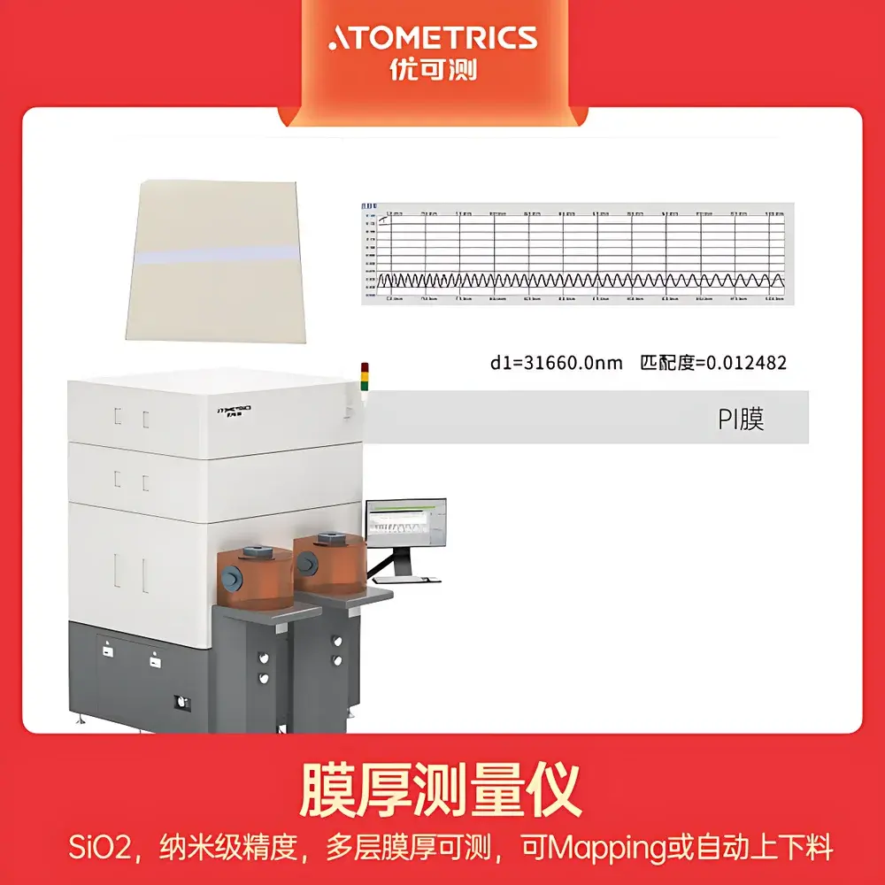
- Multi-layer capability: Supports quantitative analysis of up to 10 optically distinct layers—including transparent dielectrics (SiO₂, Al₂O₃), conductive oxides (ITO), organic polymers (PI), photoresists, liquid films, and air gaps
- High-speed acquisition: Sub-millisecond spectral capture (<10 ms per scan), enabling real-time process monitoring in inline and offline configurations
- Modular platform design: Configurable for benchtop offline use, compact inline integration (footprint <120 × 100 mm), or fully automated wafer-handling systems compatible with 100–300 mm (4–12 inch) substrates
- Surface-agnostic operation: Validated performance on roughness-varying surfaces (Rq = 0.2–50 nm) and low-reflectivity substrates (e.g., silicon wafers, glass, PET)
Sample Compatibility & Compliance
The AF-T050 accommodates diverse sample geometries and material systems common in semiconductor fabrication, display manufacturing, photovoltaics R&D, and advanced packaging. It has been validated for quantitative thickness measurement of indium tin oxide (ITO), perovskite precursors, quantum dot monolayers, spin-coated photoresists (e.g., AZ® series), polyimide (PI) passivation layers, SiO₂ dielectrics, and bonded glass interfaces. The system adheres to ISO/IEC 17025 traceability principles for optical metrology, with factory calibration traceable to NIST-certified reference standards. For regulated environments, the software architecture supports audit trails, user access control, electronic signatures, and data integrity features aligned with FDA 21 CFR Part 11 and EU Annex 11 requirements when deployed under GLP/GMP-compliant SOPs.
Software & Data Management
The AF-T050 is operated via Atometrics’ MetroSuite™ v4.2 software—a Windows-based application with dual-mode interface: wizard-driven workflow for routine QA/QC and expert mode for full model parameterization. All spectral data, fitting reports, and layer stack definitions are stored in HDF5 format with embedded metadata (wavelength calibration, lamp intensity history, environmental sensor logs). Batch processing supports statistical process control (SPC) charting (X-bar/R, Cpk), spatial mapping (via motorized XY stages), and export to CSV, XML, or industry-standard SEMI E142 (Equipment Data Acquisition) schema. Remote monitoring and configuration are enabled via TCP/IP and Modbus TCP protocols for integration into MES and SCADA systems.
Applications
- Semiconductor front-end: Monitoring ALD/CVD-grown gate oxides, hard masks, and etch-stop layers during fab process development
- Flat-panel display: In-line thickness control of ITO anodes, encapsulation barriers, and color filter stacks on TFT-LCD and OLED substrates
- Photovoltaics: Quantifying perovskite absorber layer uniformity, HTL/ETL interfacial thickness, and anti-reflective coatings on textured silicon
- Advanced packaging: Measuring redistribution layer (RDL) dielectric thickness, under-bump metallization (UBM), and bonding interface integrity in fan-out WLP
- R&D laboratories: Characterizing self-assembled monolayers (SAMs), Langmuir-Blodgett films, and solution-processed functional coatings on flexible substrates
FAQ
What is the minimum measurable thickness for ultra-thin films like ITO or perovskites?
The AF-T050 achieves reliable quantification down to 5 nm for high-contrast films (e.g., ITO on Si) and ≤10 nm for low-contrast systems (e.g., perovskite on PEDOT:PSS), with repeatability ≤±0.2 nm (3σ) under controlled environmental conditions.
Does the system support measurement on curved or non-planar substrates?
Yes—when equipped with optional auto-focus optics and tilt-compensation algorithms, the AF-T050 maintains measurement accuracy on substrates with radii ≥25 mm and surface tilts up to ±3°.
Can the AF-T050 be integrated into an existing cleanroom automation infrastructure?
Absolutely—the system provides SECS/GEM-compliant communication drivers, SECS-II message support, and hardware I/O triggers for synchronization with cluster tools, robotic handlers, and vacuum load locks.
Is spectral calibration required between measurements?
No—each lamp source is thermally stabilized and monitored in real time; factory-performed wavelength and intensity calibration remains valid for ≥12 months under standard operating conditions (20–25°C, <60% RH).
How does the segmented fitting algorithm improve accuracy over conventional full-spectrum fitting?
By decoupling dispersion modeling across spectral regions where material absorption edges dominate (e.g., bandgap transitions in perovskites), the algorithm avoids cross-band parameter coupling—reducing typical RMS fitting residuals by 40–65% compared to global Lorentzian models.


