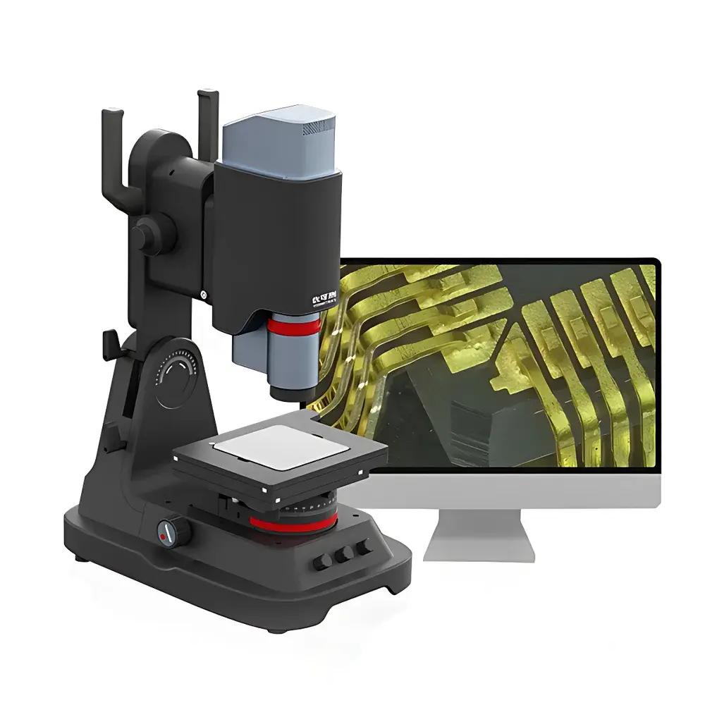
Atometrics AH Series Ultra-Deep-Field Digital Microscope
| Brand | Atometrics |
|---|---|
| Origin | Guangdong, China |
| Manufacturer Type | OEM/ODM Manufacturer |
| Country of Origin | China |
| Model Series | AH Series |
| Imaging Sensor | CMOS |
| XY Stage Dimensions | 220 mm × 180 mm |
| Frame Rate | 30 FPS |
| 3D Image Comparison Function | Yes |
| Maximum Optical Magnification | 500× |
Overview
The Atometrics AH Series Ultra-Deep-Field Digital Microscope is an industrial-grade, high-resolution optical inspection system engineered for extended depth-of-field (EDOF) imaging and quantitative 2D/3D metrology. Unlike conventional optical microscopes constrained by shallow depth of field at high magnifications, the AH Series employs multi-focus image fusion algorithms combined with precision Z-axis motorized control to synthesize fully focused composite images from a stack of focal planes. This enables consistent, distortion-free visualization and measurement across complex topographies—such as rough fracture surfaces, textured coatings, or multi-layered PCBs—without manual refocusing. Designed for integration into QC laboratories, R&D facilities, and production-line inspection stations, the system operates on a robust opto-mechanical architecture compatible with ISO 10110 optical component standards and aligned with ASTM E2926–22 guidelines for digital microscopy-based surface characterization.
Key Features
- Ultra-deep depth of field (up to 10 mm at 100×, scalable via objective lens selection), eliminating focus stacking artifacts through real-time algorithmic fusion
- Motorized Z-axis with sub-micron repeatability (±0.5 µm) and programmable step resolution down to 0.1 µm
- Integrated 12-megapixel CMOS sensor delivering 4096 × 3072 pixel resolution at full frame rate (30 FPS) in live mode
- Manual and automated XY translation stage (220 mm × 180 mm travel range) with optional encoders for traceable positional data
- One-click full-frame autofocus (<1 second acquisition time) with adaptive contrast detection optimized for low-reflectivity and heterogeneous samples
- Built-in 360° rotational sample viewing capability via motorized tilt-and-rotate stage interface (optional accessory)
- Native support for both 2D geometric measurements (distance, angle, radius, area) and 3D surface profiling (height map, volume, roughness parameters Sa/Sq per ISO 25178)
Sample Compatibility & Compliance
The AH Series accommodates specimens ranging from semiconductor wafers and metallographic cross-sections to polymer films, biological tissue sections, and electronic assemblies—without requiring conductive coating or vacuum environments. Its non-contact, visible-light illumination design complies with IEC 61000-6-3 (EMC emission limits) and meets CE marking requirements for laboratory instrumentation. All measurement workflows adhere to GLP principles: audit trails record operator ID, timestamp, calibration status, and parameter settings for each session. Optional FDA 21 CFR Part 11-compliant software modules provide electronic signatures, role-based access control, and immutable data archiving—validated for use in regulated manufacturing environments governed by ISO 9001, IATF 16949, and IPC-A-610.
Software & Data Management
The proprietary Atometrics VisionSuite v4.x platform provides unified control of imaging, metrology, and reporting functions. It supports DICOM, TIFF, PNG, and proprietary .AH3D file formats—including embedded metadata (lens ID, magnification, exposure, stage coordinates). Batch processing enables automated report generation (PDF/Excel) with customizable templates compliant with internal QA documentation standards. Raw image stacks and fused outputs are stored with SHA-256 checksums to ensure data integrity. Integration with enterprise systems is facilitated via RESTful API and OPC UA protocol support, enabling direct linkage to MES, LIMS, or PLM platforms without middleware dependency.
Applications
- Failure analysis of solder joints, wire bonds, and die attach interfaces in electronics packaging
- Surface defect classification (scratches, pits, voids, delamination) per MIL-STD-883H Method 2010
- Dimensional verification of micro-machined features (e.g., MEMS channels, medical device stents)
- Material grain structure assessment and phase distribution mapping in metallurgical samples
- Coating thickness estimation via edge-detection assisted cross-sectional reconstruction
- Non-destructive evaluation of additive manufacturing build layers and porosity distribution
FAQ
Does the AH Series support calibration traceability to national standards?
Yes—certified reference standards (NIST-traceable step height, line width, and pitch artifacts) are available for routine performance verification. Calibration certificates include uncertainty budgets per ISO/IEC 17025.
Can third-party lenses be mounted on the AH microscope body?
The system uses a standardized C-mount interface and supports interchangeable objectives (0.5×–5× telecentric, long-working-distance, and infinity-corrected lenses) from major suppliers including Navitar, Edmund Optics, and Mitutoyo.
Is real-time 3D rendering supported during live acquisition?
No—3D surface reconstruction requires post-acquisition stack processing; however, preview mode displays dynamic focus tracking and estimated depth map overlays in near real time.
What is the maximum specimen height clearance under the objective?
With standard configuration and 1× objective, vertical working distance is 120 mm; optional extended-Z columns increase clearance to 250 mm.
How is firmware updated and version history maintained?
Updates are delivered via secure HTTPS download with cryptographic signature validation. All firmware revisions are logged in the system event database with rollback capability and change impact documentation.


