Atometrics AP-5005 Spectral Confocal Displacement Sensor
| Brand | Atometrics |
|---|---|
| Model | AP-5005 |
| Origin | Guangdong, China |
| Manufacturer Type | Original Equipment Manufacturer (OEM) |
| Country of Origin | China |
| Pricing | Upon Request |
Overview
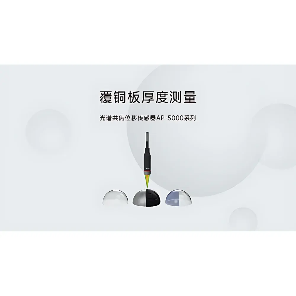
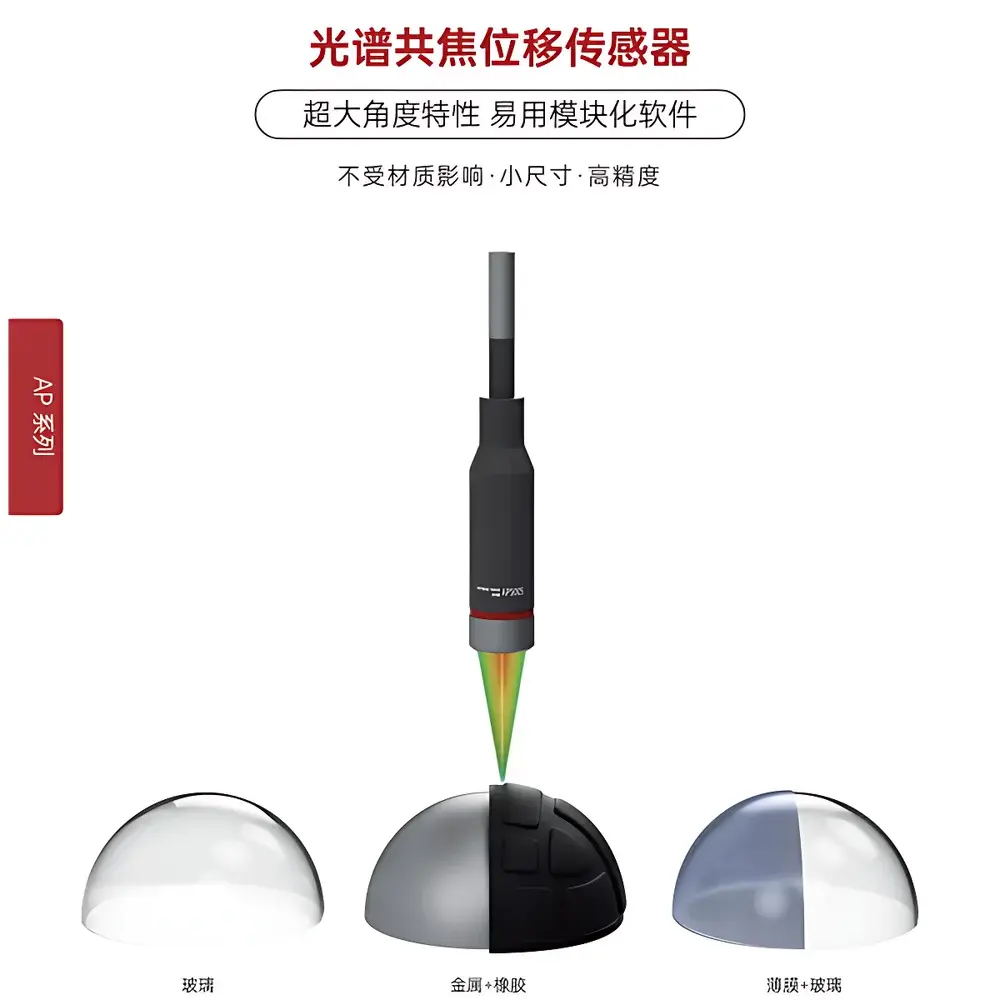
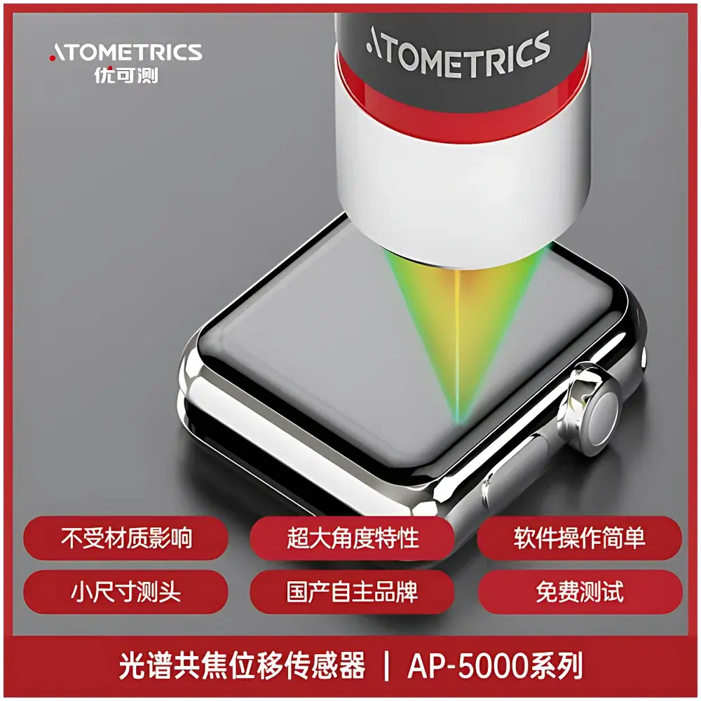
The Atometrics AP-5005 Spectral Confocal Displacement Sensor is a high-precision non-contact metrology instrument engineered for sub-micron vertical displacement and surface topography measurement. It operates on the principle of spectral confocal microscopy: a broadband white-light point source is focused through a chromatic lens assembly, where axial position is encoded as wavelength due to controlled axial chromatic aberration. Light reflected from the target surface re-enters the optical path and is dispersed spectrally by a diffraction grating onto a CMOS linear spectrometer array. The peak wavelength corresponding to maximum intensity is uniquely mapped to the object’s axial position with nanometer-level resolution—enabling absolute distance measurement without mechanical scanning or calibration drift. Designed for integration into automated inspection systems, the AP-5005 delivers high repeatability (<±50 nm), excellent linearity (≤0.1% FS), and immunity to surface reflectivity, transparency, or color variations—making it suitable for demanding applications in semiconductor fabrication, precision optics, medical device manufacturing, and battery production.
Key Features
- Spectral confocal architecture enabling true single-point, absolute height measurement without reference surfaces or zeroing procedures
- High axial resolution down to 10 nm (typical) and repeatability better than ±50 nm across full measurement range
- Robust optical design with integrated fiber-coupled illumination and detection path—minimizing alignment sensitivity and environmental drift
- Wide dynamic range: standard measurement ranges include ±0.5 mm, ±1 mm, and ±2 mm (custom ranges available)
- Real-time analog output (0–10 V) and digital interface (RS-422 or Ethernet TCP/IP) for seamless OEM system integration
- Compact, industrial-grade housing rated IP64 for operation in cleanroom and factory-floor environments
- No moving parts—ensuring long-term stability and maintenance-free operation over >50,000 hours MTBF
Sample Compatibility & Compliance
The AP-5005 reliably measures surfaces regardless of material composition—including transparent (glass, sapphire, polymer films), reflective (silicon wafers, polished metals), scattering (ceramics, anodized aluminum), or multi-layer structures (coated lenses, battery electrode stacks). Its insensitivity to surface finish eliminates the need for specular reflection or diffuse coating—a key advantage over laser triangulation sensors. The sensor complies with IEC 61326-1 (EMC for industrial environments) and meets CE marking requirements. For regulated industries, raw data export supports traceability under ISO 9001, ISO/IEC 17025, and FDA 21 CFR Part 11 when paired with compliant host software featuring audit trail, electronic signatures, and data integrity controls.
Software & Data Management
Atometrics provides the Atoscan Control Suite—a Windows-based application supporting real-time waveform display, multi-sensor synchronization, XY scanning trajectory definition, and batch report generation (PDF/CSV/XLSX). The SDK includes C/C++, .NET, and LabVIEW APIs for custom integration into PLC-controlled platforms or MES/QMS ecosystems. All measurement data is timestamped and tagged with sensor ID, environmental metadata (optional external temperature/humidity input), and operator credentials. Raw spectral profiles are preserved for retrospective analysis and uncertainty budgeting per GUM (JCGM 100:2018). Optional cloud-enabled firmware updates and remote diagnostics support Industry 4.0 readiness.
Applications
- Semiconductor: Wafer bow and thickness mapping, die attach coplanarity, probe card pin height verification, TSV depth profiling
- Battery Manufacturing: Anode/cathode coating thickness uniformity, jelly-roll compression monitoring, pouch cell swelling quantification
- Optics & Glass: Lens surface form error (spherical/aspheric), glass substrate thickness variation, AR-coating layer stack metrology
- Medical Devices: Syringe barrel wall thickness, dental implant thread pitch and flank angle, IV bag film thickness consistency
- Consumer Electronics: OLED panel curvature (R-value), button tactile travel, camera module lens tilt and focus gap
- Precision Engineering: Spindle axial runout, bearing raceway waviness, micro-gear tooth profile deviation
FAQ
What is the minimum measurable feature size?
The AP-5005 resolves lateral features ≥5 µm when used with appropriate focusing optics; axial resolution is independent of spot size and remains ≤10 nm.
Can it measure transparent multilayer films?
Yes—the spectral confocal method detects individual interfaces within transparent stacks (e.g., PET/ITO/glass) by resolving multiple spectral peaks corresponding to each boundary.
Is vacuum or inert gas compatibility available?
Standard units operate at ambient pressure; custom hermetic housings with CF flanges and quartz windows are offered for UHV (<10⁻⁶ mbar) and glovebox integration.
How does temperature affect measurement stability?
The sensor exhibits <0.02% FS/°C thermal drift; optional internal temperature compensation algorithms reduce this to <0.005% FS/°C using onboard thermistor feedback.
Does it require periodic recalibration?
No—spectral confocal geometry is inherently self-referencing; NIST-traceable verification is recommended annually per ISO/IEC 17025 guidelines, not mandatory recalibration.


