Atometrics T100 Optical Thin Film Metrology System
| Brand | Atometrics |
|---|---|
| Origin | Guangdong, China |
| Manufacturer Type | OEM Manufacturer |
| Regional Classification | Domestic (China) |
| Model | T100 |
| Pricing | Upon Request |
Overview
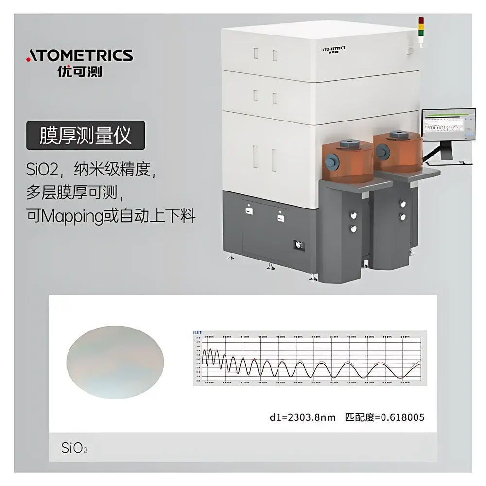
The Atometrics T100 Optical Thin Film Metrology System is a precision spectroscopic reflectometry platform engineered for non-contact, real-time measurement of thin film thickness and optical constants (n, k) across semiconductor process development, R&D, and high-volume manufacturing environments. Based on broadband spectral reflectance analysis—spanning the deep ultraviolet (DUV) to near-infrared (NIR) range—the T100 employs a dual-light-source architecture (deuterium lamp: 180–370 nm; tungsten-halogen lamp: 320–2400 nm) to ensure high signal-to-noise ratio and spectral continuity across critical absorption edges of common functional layers (e.g., ITO, perovskites, quantum dots, SiO₂, PI, photoresists). Unlike conventional single-band or LED-based systems, the T100 implements a proprietary segmented spectral fitting algorithm that partitions the full spectrum into physically meaningful wavelength sub-bands—each independently weighted and constrained by material dispersion models—thereby minimizing fitting ambiguity and significantly reducing residual error in multilayer stack inversion. This approach delivers sub-angstrom (≤0.1 nm) thickness resolution on monolayers and enables robust characterization of complex stacks with interfacial roughness, grading, or optical anisotropy.
Key Features
- Dual broadband illumination: Deuterium lamp (180–370 nm) + tungsten-halogen lamp (320–2400 nm), enabling seamless coverage from DUV through NIR without spectral gaps or intensity roll-off
- Segmented spectral fitting engine: Physically informed, multi-band regression algorithm that improves model convergence and reduces parameter correlation in multilayer optical modeling
- High-speed acquisition: Sub-100 ms spectral capture per measurement point—optimized for inline integration and rapid wafer mapping
- Modular configuration options: Supports offline benchtop, inline OEM integration (compact footprint, USB 3.0 interface), and fully automated wafer-handling versions compatible with 100–300 mm (4–12 inch) substrates
- Robust optical design: Fixed-focus probe head with fiber-coupled optics, temperature-stabilized detector array, and active reference channel for long-term photometric stability
Sample Compatibility & Compliance
The T100 is validated for use on planar and patterned substrates including silicon wafers, glass carriers, fused silica, sapphire, and flexible polymer films. It supports single-layer and multilayer structures composed of dielectrics (SiO₂, Si₃N₄, Al₂O₃), transparent conductive oxides (ITO, AZO), organic semiconductors (perovskites, QDs), polymers (PI, BCB, photoresists), and metal films (Ti, Cr, Al, Cu) down to sub-nanometer thicknesses. Measurement protocols align with industry-standard optical modeling conventions defined in ASTM E1936 (Standard Guide for Spectroscopic Ellipsometry and Reflectometry), ISO/IEC 17025 (for calibration traceability), and SEMI E172 (Specification for Optical Metrology Equipment in Semiconductor Manufacturing). The system’s software architecture supports audit trail logging and user access control per FDA 21 CFR Part 11 requirements when deployed in regulated GMP/GLP environments.
Software & Data Management
The T100 is operated via Atometrics’ MetroSuite™ v4.x software—a Windows-based application built on .NET Framework with native support for instrument control, optical modeling (using Cauchy, Sellmeier, Tauc-Lorentz, and Cody-Lorentz dispersion functions), and database-driven recipe management. All measurement data—including raw spectra, fitted parameters, confidence intervals, and residual plots—are stored in vendor-neutral HDF5 format with embedded metadata (wavelength calibration, lamp status, environmental conditions). MetroSuite integrates with factory automation standards including SECS/GEM and PV2 via TCP/IP, and provides RESTful API endpoints for custom MES/SPC integration. Full version history, electronic signatures, and change logs are maintained for compliance with ISO 9001 and internal QA workflows.
Applications
- Process development and qualification of ALD, PVD, CVD, and spin-coated thin films in semiconductor front-end and advanced packaging lines
- In-line monitoring of anti-reflective coatings, passivation layers, and barrier films on display and photovoltaic substrates
- R&D of emerging optoelectronic materials—including perovskite solar cells, microLED encapsulation layers, and quantum dot color conversion films
- Quality assurance of MEMS and microfluidic devices where precise etch depth and bonding layer uniformity are critical
- Failure analysis and root cause investigation of delamination, interdiffusion, and oxidation-induced thickness drift
FAQ
What wavelength range does the T100 cover, and how is spectral continuity ensured?
The T100 uses synchronized deuterium (180–370 nm) and tungsten-halogen (320–2400 nm) sources with overlapping output in the 320–370 nm region, eliminating blind spots and ensuring continuous, high-fidelity reflectance data across the entire operational band.
Can the T100 measure ultra-thin films (<1 nm) or buried interfaces?
Yes—when combined with appropriate optical models and sufficient spectral signal-to-noise, the T100 resolves sub-Å thickness changes in monolayer adsorbates and detects interfacial oxide growth or intermixing via subtle shifts in interference minima and dispersion behavior.
Is the system compatible with cleanroom Class 100/ISO 5 environments?
The inline and automated configurations are designed for Class 100 compatibility, featuring sealed optical paths, low-outgassing materials, and ESD-safe enclosures compliant with SEMI S2/S8 safety guidelines.
Does the software support custom optical models or third-party modeling libraries?
MetroSuite™ allows import of user-defined dispersion models via DLL interface and supports direct export of spectra and fit parameters to MATLAB, Python (NumPy/SciPy), and commercial tools such as Woollam CompleteEASE and SENTECH SOPRA.
How is calibration traceability maintained over time?
The system includes NIST-traceable reflectance standards (Si/SiO₂ wafers with certified thickness values) and supports automated daily verification routines with drift compensation algorithms logged in the audit trail.


