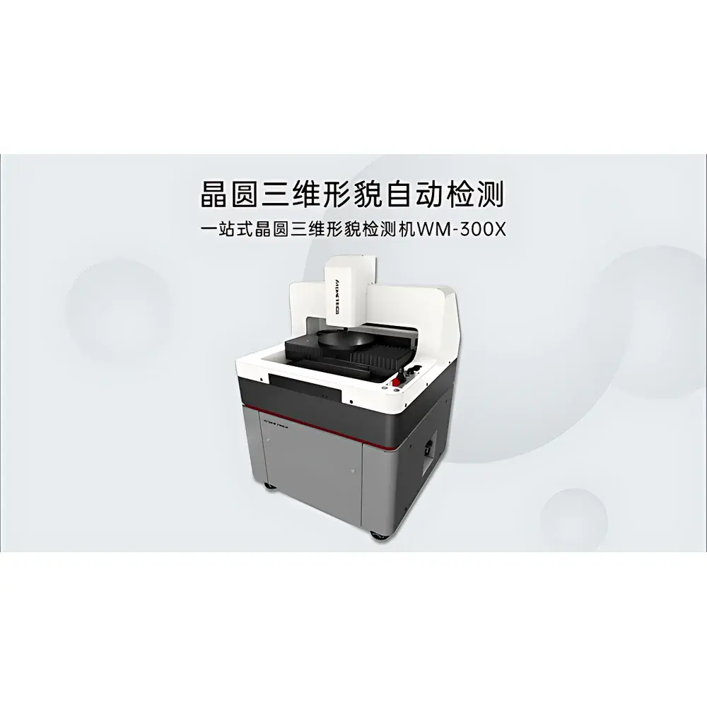
Atometrics WM300R Advanced Wafer 3D Profilometer
| Brand | Atometrics |
|---|---|
| Origin | Guangdong, China |
| Manufacturer Type | OEM/ODM Producer |
| Country of Origin | China |
| Model | WM300R |
| Pricing | Upon Request |
Overview
The Atometrics WM300R is a high-precision, non-contact optical profilometer engineered for comprehensive 3D surface topography characterization of semiconductor wafers and precision optics. It operates on the principle of vertical scanning white-light interferometry (VSI), delivering nanometer-scale vertical resolution and sub-micrometer lateral sampling across large fields of view. Designed specifically for front-end and back-end semiconductor process control—including grinding, thinning, etching, scribing, bumping, and mask inspection—the WM300R meets the stringent metrology demands of 300 mm (12-inch) wafer fabrication environments. Its modular architecture integrates a research-grade monochrome CMOS imaging sensor, piezoelectric Z-scanner with 5000 µm vertical range, and interchangeable interference objectives (2.5× to 100×), enabling adaptive measurement configurations for both macro-scale step height analysis and nanoscale roughness quantification.
Key Features
- Vertical resolution down to 0.03 nm RMS, validated per ISO 25178-2:2012 and ISO 4287:1997 standards
- Maximum measurable step height: 5000 µm with accuracy of ±0.3% of measured value
- High-speed VSI scanning: up to 400 µm/s vertical scan velocity; platform XY travel at 300 mm/s
- 2.3 MP monochrome CMOS sensor (1920 × 1200 pixels), high quantum efficiency, frame rates from 169 Hz to 3200 Hz
- Nanopositioning Z-stage based on piezoelectric ceramic actuator—5000 µm full range (400 µm high-resolution mode optional)
- Vacuum chuck with one-touch activation, compatible with 100–300 mm (4–12 inch) wafers, VC-D grade vibration isolation
- Interchangeable interference objectives: 2.5×, 5×, 10×, 20×, 50×, and 100× magnifications for optimized field-of-view and resolution trade-offs
Sample Compatibility & Compliance
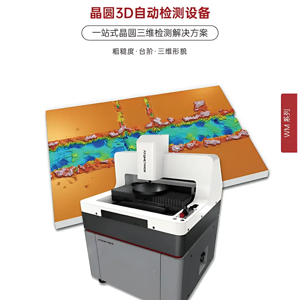
The WM300R supports broad sample classes critical to semiconductor manufacturing: silicon wafers (bare, polished, patterned, or coated), photomasks, reticles, MEMS substrates, and bump structures. Its measurement algorithms comply with international surface texture standards—including ISO 25178 series (areal surface texture parameters such as Sq, Sa, Sz) and ISO 4287 (profile-based roughness parameters). The system is designed for integration into GLP- and GMP-aligned QA/QC workflows; raw data logging, audit trails, and user-access controls support compliance readiness for FDA 21 CFR Part 11 where software validation is implemented per customer requirements.
Software & Data Management
The proprietary Atometrics ProfilSoft™ platform provides intuitive, script-free operation: automated measurement sequencing, real-time 3D rendering, and standardized reporting compliant with ISO 25178 and ISO 4287. Key capabilities include batch measurement programming, automatic report generation (PDF/CSV), advanced 3D surface analysis (cross-section extraction, volume calculation, slope mapping), and SDK-based customization for factory automation (SECS/GEM, OPC UA compatibility available upon request). Embedded SST (Smart Surface Tracking) and GAT (Gradient-Accelerated Tomography) algorithms accelerate data reconstruction without compromising fidelity—enabling full-wafer scans in under 90 seconds at 0.6 µm lateral sampling.
Applications
- Quantitative evaluation of grinding and thinning uniformity across 300 mm wafers
- Etch depth profiling and sidewall angle assessment on patterned Si, SiO₂, and low-k dielectrics
- Mask and reticle defect depth characterization (e.g., chrome layer erosion, quartz pit depth)
- Bump height, coplanarity, and solder joint geometry analysis for flip-chip and 2.5D/3D IC packaging
- Surface finish verification post-CMP, laser ablation, or plasma treatment
- Research-grade surface morphology studies requiring areal roughness (Sa, Sq, Sdr) and functional parameters (Sk, Spk, Svk)
FAQ
What surface parameters does the WM300R calculate per ISO 25178?
It computes all primary areal parameters including Sa (arithmetic mean height), Sq (root-mean-square height), Sz (maximum height), Sdr (developed interfacial area ratio), and functional parameters such as Sk (core roughness depth), Spk (reduced peak height), and Svk (reduced valley depth).
Is the system compatible with automated fab environments?
Yes—the platform supports SECS/GEM communication protocols and offers SDK access for integration into MES and APC systems; vacuum chuck and VC-D isolation ensure stability in high-throughput cleanroom settings.
Can the WM300R measure transparent or highly reflective surfaces?
Yes—adaptive coherence gating and polarization control in the interferometric path enable robust measurement on bare silicon, SiO₂ films, metalized layers, and low-reflectivity anti-reflective coatings.
Does the software support custom report templates and export formats?
Yes—users may define report layouts with embedded images, statistical summaries, and pass/fail thresholds; outputs include PDF, CSV, X3P, and STP for CAD interoperability.
What calibration standards are recommended for routine verification?
NIST-traceable step height standards (e.g., NIST SRM 2160, 2161) and roughness standards (e.g., NIST SRM 2162) are recommended; system-level verification follows ISO 25178-601 procedures.