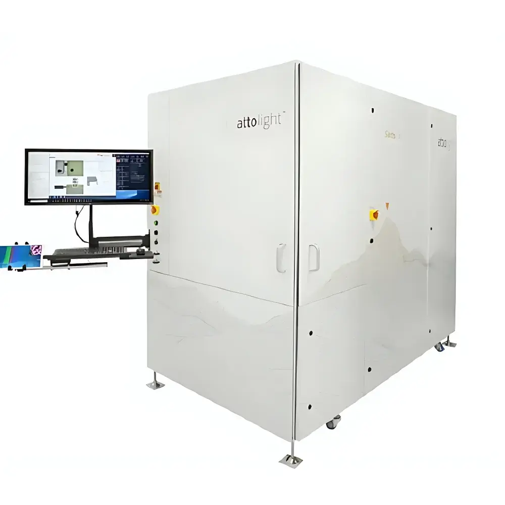
Attolight Santis 300 Full-Wafer Industrial Cathodoluminescence SEM System
| Brand | Attolight |
|---|---|
| Origin | Switzerland |
| Model | Santis 300 |
| Wafer Handling | Fully automated for 150 mm, 200 mm, and 300 mm wafers |
| Positioning Accuracy | <10 µm |
| Warpage Compensation | Real-time topography mapping and stage tilt correction |
| Acquisition Modes | Full-Field Brush (FWBrush), Averaged Pixel (AWPix), and Multi-Point Spot Scanning |
| CL Spectral Range | Typically 200–1100 nm (configurable with grating options) |
| Detector | Back-illuminated CCD or sCMOS with high quantum efficiency in UV-VIS-NIR |
| Integration with SEM | Synchronized electron beam scanning and photon collection via fiber-coupled monochromator or spectrometer |
Overview
The Attolight Santis 300 is a fully integrated, industrial-grade cathodoluminescence scanning electron microscope (CL-SEM) system engineered for quantitative, large-area optical characterization of semiconductor wafers up to 300 mm in diameter. Unlike conventional CL systems requiring manual sample alignment or limited field-of-view stitching, the Santis 300 employs a robust, motorized wafer handling platform combined with real-time electron-beam–photon-signal synchronization to deliver simultaneous acquisition of high-resolution SEM topography, spatially resolved cathodoluminescence intensity maps, and point-spectrum or hyperspectral CL data across the entire wafer surface. Its core measurement principle relies on electron-induced luminescence: when a focused electron beam impinges on a semiconductor, it generates electron-hole pairs whose radiative recombination emits photons characteristic of local band structure, defect states, strain, composition, and crystallinity. This enables nanoscale correlative analysis—linking structural features observed in SEM directly to their optoelectronic signatures—without physical relocation or signal degradation from repeated vacuum cycles.
Key Features
- Fully automated wafer handling for 150 mm, 200 mm, and 300 mm substrates—including standard notch/flat recognition and edge detection with sub-10 µm repeatability
- Integrated warpage mapping: uses capacitive or laser triangulation sensors to reconstruct wafer surface topography prior to scanning, then dynamically adjusts stage tilt and focus during acquisition to maintain optimal beam-sample interaction
- Three configurable acquisition modes: FWBrush (full-field raster for rapid overview CL imaging), AWPix (line-scanned averaged pixel mode for improved signal-to-noise in low-emission materials), and Multi-Point Spot (targeted spectroscopy at user-defined coordinates)
- Synchronized dual-channel detection: simultaneous capture of secondary electron (SE) and backscattered electron (BSE) signals alongside time-gated or continuous CL photons via fiber-optic coupling to a high-throughput monochromator or imaging spectrometer
- Modular optical path: supports interchangeable gratings, filters, and detectors to optimize spectral resolution (down to 0.1 nm), wavelength range (UV–NIR), and quantum efficiency per application requirement
- Industrial-grade vacuum architecture: compatible with standard cleanroom SEM integration protocols and designed for >8,000 hours mean time between failures (MTBF) under continuous production use
Sample Compatibility & Compliance
The Santis 300 accommodates bare and processed wafers—including patterned GaN-on-sapphire, SiC-on-Si, GaAs-based heterostructures, and micro-LED arrays—with minimal preparation requirements. It supports both conductive and semi-insulating substrates; charge compensation is achieved via low-energy flood gun or beam current modulation. The system complies with ISO 14644-1 Class 5 cleanroom compatibility standards and meets electromagnetic compatibility (EMC) requirements per IEC 61326-1. For regulated environments, optional audit-trail logging, user access control, and electronic signature support align with FDA 21 CFR Part 11 and EU Annex 11 expectations when deployed in GLP/GMP-aligned R&D or process validation workflows.
Software & Data Management
Control and analysis are performed via Attolight’s CLARITY™ software suite—a deterministic, scriptable platform built on Qt and Python APIs. It provides real-time visualization of SEM + CL overlays, batch processing of hyperspectral cubes (e.g., PCA, cluster analysis, band-edge fitting), and export to standardized formats (HDF5, TIFF, MRC). All raw and processed datasets are timestamped, metadata-tagged (beam energy, dwell time, aperture, grating position), and stored in a hierarchical directory structure compliant with FAIR data principles. Optional integration with MES or LIMS systems is supported via RESTful API or OPC UA protocol.
Applications
- Quantitative defect metrology: threading dislocation density mapping in GaN epitaxial layers using CL peak-width and intensity variance analysis—correlated to device yield and lifetime predictions
- UVC LED uniformity assessment: full-wafer CL intensity homogeneity evaluation at 275 nm, enabling statistical process control (SPC) for sterilization-grade emitters
- SiC substrate quality screening: identification and classification of micropipes, basal plane dislocations, and polytype inclusions via spectral fingerprinting and spatial correlation with BSE contrast
- Micro-LED array characterization: pixel-level efficiency, emission wavelength shift, and non-radiative recombination hotspot localization across 12-inch GaN-on-silicon wafers
- Photonic crystal cavity optimization: resonant mode mapping and Q-factor estimation through angle-resolved CL spectroscopy on patterned III–V platforms
- Strain and composition profiling in InGaN quantum wells: using peak energy shifts and linewidth broadening in calibrated CL spectra to infer local indium content and biaxial stress distribution
FAQ
Does the Santis 300 require modification of my existing SEM column?
No—the system integrates as a side-mounted, UHV-compatible optical module using standard flange interfaces (CF100 or CF160); no electron optics alterations are needed.
Can CL data be correlated with EBSD or EDX maps acquired on the same instrument?
Yes—CLARITY™ supports co-registration of CL, SEM, EBSD, and EDX datasets using common fiducial markers or geometric transformation matrices derived from stage encoder feedback.
Is the system qualified for use in ISO Class 5 cleanrooms?
Yes—mechanical design, material selection (electropolished stainless steel, low-outgassing elastomers), and cabling meet ISO 14644-1 Class 5 particulate and outgassing specifications.
What level of spectral calibration traceability is provided?
Each spectrometer is factory-calibrated against NIST-traceable Hg/Ar emission lines; users receive a calibration certificate with uncertainty budget per ISO/IEC 17025.
How is data integrity ensured during long-duration full-wafer scans?
Real-time checksum verification, redundant storage buffering, and automatic resume-after-interruption functionality prevent data loss during power fluctuations or network latency events.