Auniontech AU-TRSD103 In-Plane Thermal Conductivity Measurement System
| Brand | Auniontech |
|---|---|
| Origin | Shanghai, China |
| Model | AU-TRSD103 |
| Measurement Principle | Optical AC Calorimetry (Pump-Probe Frequency-Domain Thermoreflectance) |
| Laser Wavelengths | Pump 638 nm, Probe 785 nm (standard) |
| Pump Power | 100 mW |
| Probe Power | 20 mW |
| Modulation Frequency Range | DC–5 kHz (upgradable to 200 MHz) |
| Spot Size (1/e²) | ~15 µm (with 10× objective) |
| Thermal Conductivity Range (in-plane) | 0.05–5000 W/(m·K) |
| Measurement Uncertainty | ≤5% for in-plane κ, ≤10% for volumetric heat capacity |
| Sample Diameter Minimum | ≥50 µm |
| Surface Roughness Requirement | ≤15 nm RMS |
| Temperature Range | Ambient (upgradable to 4–1200 K) |
| Data Acquisition Time per Measurement | ≤2 min |
| Spatial Resolution (imaging mode) | 1 µm |
| Compliance | GLP-ready data audit trail, ISO/IEC 17025-aligned calibration traceability |
Overview
The Auniontech AU-TRSD103 In-Plane Thermal Conductivity Measurement System is a benchtop optical platform engineered for high-precision, non-contact characterization of in-plane thermal transport properties in solid-state materials. It implements an advanced implementation of frequency-domain thermoreflectance (FDTR) based on optical AC calorimetry—specifically, a dual-beam pump-probe architecture operating in the spatial and temporal frequency domains. Unlike conventional steady-state or time-domain methods, the AU-TRSD103 extracts thermal diffusivity and conductivity by analyzing both amplitude decay and phase lag of surface temperature oscillations induced by intensity-modulated pump light, while simultaneously monitoring thermoreflectance changes via a spatially offset probe beam. This dual-signal (phase + normalized amplitude) inversion enables robust, model-based fitting of in-plane thermal conductivity κ∥, volumetric heat capacity Cv, and interfacial thermal resistance Rint, without requiring prior knowledge of substrate cross-plane conductivity or metal transducer layer thermal parameters. The system is fundamentally designed for research-grade metrology in thin films, microstructured devices, and anisotropic crystals—where lateral heat flow dominates device-level thermal management.
Key Features
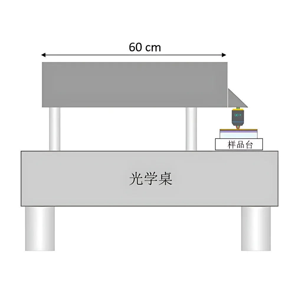
- Optically isolated, black-box enclosure (60 cm × 60 cm footprint) with integrated dust shielding and laser safety interlocks (Class 1 compliant when closed)
- Dual-wavelength continuous-wave laser configuration: 638 nm pump (100 mW), 785 nm probe (20 mW), enabling high signal-to-noise thermoreflectance detection on Ti, Al, or Au transducer layers
- Balanced photodetector architecture minimizing low-frequency drift and enabling sub-second lock-in acquisition per measurement point
- Simultaneous joint fitting of in-plane thermal conductivity and effective laser spot size (1/e²), decoupling optical uncertainty from thermal parameter extraction
- Automated phase calibration and real-time noise compensation—eliminating manual reference-phase adjustment required in conventional FDTR
- Motorized microscope stage with CCD live imaging (10× standard objective; optional 2×–50× zoom and auto-switching turret) for precise sample alignment and spot positioning
- Modular thermal environment support: ambient baseline configuration with field-upgrade paths to cryogenic (4–300 K), high-temperature (300–1200 K), or wide-range (80–500 K) stages
- Full software control of modulation frequency sweep (DC–5 kHz standard; up to 200 MHz), power ramping, focus optimization, and multi-point raster scanning
Sample Compatibility & Compliance
The AU-TRSD103 accommodates planar samples ranging from ultrathin films (≥100 nm) to bulk wafers, provided surface roughness remains ≤15 nm RMS over the measurement area (typically ≥100 µm diameter). Minimal sample diameter is 50 µm—enabled by micron-scale optical focusing. Transducer layers must be optically opaque at the pump wavelength (high absorption α > 10⁵ m⁻¹) and exhibit strong thermoreflectance contrast at the probe wavelength (ΔR/R > 10⁻⁵/K). Standard 100 nm Ti or Al films satisfy these criteria across common semiconductor and dielectric substrates. For highly anisotropic or low-κ materials (e.g., polymers, oxides), transducer thermal conductivity must not exceed 10× that of the underlying sample to maintain sensitivity to in-plane phonon transport. All measurements adhere to ISO 18434-1 (condition monitoring — thermography) foundational principles and support GLP-compliant documentation through timestamped, versioned raw data archives with full metadata (laser power, modulation frequency, spot position, ambient conditions). Audit trails comply with FDA 21 CFR Part 11 requirements when configured with electronic signature modules.
Software & Data Management
The proprietary AU-TRSD Control Suite provides fully automated experiment sequencing—from autofocus and coarse alignment to multi-frequency sweep acquisition and inverse modeling. Raw lock-in outputs (X, Y, R, θ) are stored in HDF5 format with embedded calibration coefficients and instrument configuration logs. Thermal parameter extraction uses a rigorously validated finite-element forward model coupled with Levenberg-Marquardt optimization, supporting simultaneous inversion of κ∥, Cv, and Rint. Batch processing enables statistical analysis across wafer maps or material libraries. Export options include CSV, MATLAB .mat, and PDF reports with uncertainty propagation (Monte Carlo-based error estimation). Software architecture supports remote operation via secure SSH tunneling and integrates with LabVIEW and Python APIs (PyAU-TRSD) for custom workflow automation and third-party data pipeline ingestion.
Applications
- Quantitative mapping of in-plane thermal anisotropy in 2D materials (graphene, MoS₂, h-BN), ferroelectric oxides, and layered perovskites
- Thermal interface resistance quantification at metal/dielectric, polymer/ceramic, and heteroepitaxial junctions in advanced packaging
- Process development feedback for ALD/CVD-grown thermal barrier coatings, transparent conductive oxides, and flexible electronics substrates
- Validation of ab initio lattice dynamics simulations and phonon Boltzmann transport equation (BTE) solvers
- High-throughput screening of thermoelectric thin-film candidates (ZT optimization via κ∥/σ ratio tracking)
- Reliability assessment of micro-LED arrays, GaN HEMTs, and silicon photonics waveguides under thermal stress
FAQ
What minimum sample thickness can the AU-TRSD103 characterize?
The system measures in-plane thermal transport independent of substrate thickness; films as thin as 100 nm are fully supported, provided a continuous, adherent transducer layer is deposited.
Is vacuum or inert atmosphere required during measurement?
No—ambient air operation is standard. Optional environmental chambers (N₂-purged or vacuum-compatible) are available for oxidation-sensitive samples.
Can the system resolve thermal anisotropy in crystalline materials?
Yes. By rotating the sample stage in 1° increments and acquiring angular-dependent phase/amplitude data, the full 2×2 in-plane thermal conductivity tensor κxx, κyy, κxy is reconstructed without assuming isotropy.
How is calibration traceability maintained?
Primary calibration uses NIST-traceable thermoreflectance standards (Si/SiO₂ reference wafers) and secondary verification against certified bulk Si and sapphire reference samples measured per ASTM E1461.
Does the software support automated pass/fail thresholding for production QA?
Yes—customizable QC templates allow defining κ∥ upper/lower limits, Cv tolerances, and Rint acceptance bands, with real-time flagging and export to MES systems via OPC UA.


