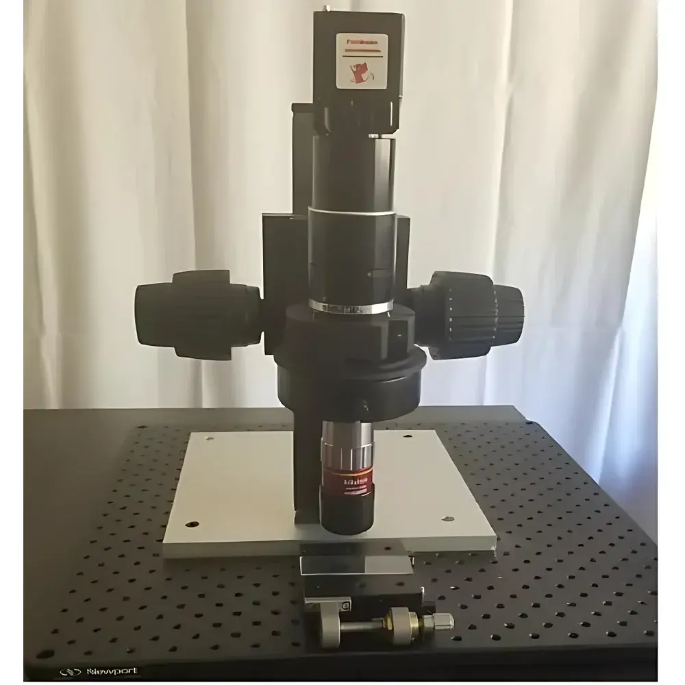
Auniontech SWIR Infrared Optical Microscope
| Brand | Auniontech |
|---|---|
| Model | SWIR |
| Imaging Range | Short-Wave Infrared (900–1700 nm) |
| Magnification | 67× to 1000× |
| Illumination Options | Coaxial LED, Laser, Broadband Sources |
| Configuration Types | Upright & Horizontal |
| Dual-Channel Capability | Yes |
| Application Focus | Semiconductor Inspection, In Vivo SWIR Fluorescence Imaging, Forensic Analysis, Cultural Heritage Examination |
| Compliance | Designed for ISO/IEC 17025-aligned lab environments, supports GLP/GMP documentation workflows |
Overview
The Auniontech SWIR Infrared Optical Microscope is a precision-engineered imaging platform optimized for short-wave infrared (SWIR) spectral band visualization—spanning 900 nm to 1700 nm. Unlike conventional visible-light microscopes, this system leverages SWIR photon detection to reveal subsurface structural features, material-specific absorption contrasts, and fluorescence signatures inaccessible to visible or near-infrared (NIR) systems. Its optical architecture integrates high-transmission SWIR-grade objectives, anti-reflection-coated beam paths, and thermoelectrically stabilized InGaAs focal plane array (FPA) detection—enabling high signal-to-noise ratio imaging under low-light or scattering-rich conditions. The microscope is not a fixed-form instrument but a modular platform: core components—including objective turrets, illumination modules, sample stages, and detector interfaces—are selected and calibrated per application-specific requirements, ensuring optimal resolution, working distance, field of view (FOV), and depth-of-field trade-offs.
Key Features
- Configurable magnification range from 67× to 1000× via interchangeable SWIR-optimized objective lenses (e.g., 10×, 20×, 50×, 100×), each corrected for chromatic and spherical aberration across the 900–1700 nm band
- Dual-channel imaging capability supporting simultaneous or sequential acquisition in two discrete SWIR sub-bands—enabling ratiometric analysis, spectral unmixing, or multi-excitation fluorescence discrimination
- Coaxial illumination architecture with selectable sources: high-stability SWIR LEDs (centered at 1064 nm or 1310 nm), pulsed or CW lasers (e.g., 1064 nm Nd:YAG or 1550 nm fiber lasers), and broadband thermal emitters—each integrated with neutral density filtering and intensity feedback control
- Horizontal (inverted-style) and upright configurations available; horizontal layout accommodates large, irregular, or heat-sensitive samples—common in semiconductor wafer metrology and packaged IC inspection
- Motorized XYZ stage with 100 mm travel range, 1 µm repeatability, and programmable coordinate mapping—compatible with automated defect scanning protocols per SEMI standards
- Modular mechanical design supports future upgrades including polarization-resolved imaging, time-resolved fluorescence lifetime attachment (TCSPC-ready interface), or integration with FTIR spectrometers
Sample Compatibility & Compliance
The SWIR microscope accommodates diverse sample geometries and physical states: planar semiconductor wafers (Si, GaAs, InP, SiC), biological tissues (ex vivo slices, in vivo murine models), polymer composites, historical artifacts (parchment, pigments, varnishes), and forensic trace evidence (fibers, gunshot residue, latent fingerprints on non-porous substrates). All optical coatings and lens materials meet MIL-PRF-13830B scratch-dig specifications. System calibration procedures align with ISO 10110-5 (surface form tolerances) and ASTM E2594 (standard practice for quantitative SWIR imaging). For regulated environments, the platform supports audit-trail logging, user-access controls, and electronic signature capture—facilitating compliance with FDA 21 CFR Part 11, EU Annex 11, and GLP/GMP documentation frameworks.
Software & Data Management
Acquisition and analysis are managed through Auniontech’s proprietary SWIRVision Suite—a Qt-based application with Python API extension support. Core functionalities include real-time image stacking, drift-corrected time-lapse acquisition, region-of-interest (ROI) intensity profiling, spectral ratio mapping (e.g., I1310nm/I1550nm), and batch-mode annotation for defect classification. Raw data is stored in HDF5 format with embedded metadata (wavelength, exposure, objective ID, stage coordinates, illumination settings). Export options include TIFF (16-bit linear), CSV (intensity/time series), and DICOM-SWIR-compliant containers for PACS integration in preclinical imaging facilities. Software validation documentation (IQ/OQ/PQ templates) is provided for laboratory accreditation purposes.
Applications
- Semiconductor Process Control: Detection of subsurface voids, delamination, and dopant distribution in silicon-on-insulator (SOI) wafers and compound semiconductor devices—leveraging SWIR transparency of silicon up to ~1100 nm and enhanced contrast at longer wavelengths for buried metal layers
- In Vivo Preclinical Imaging: Longitudinal SWIR fluorescence tracking of indocyanine green (ICG), rare-earth nanoprobes (e.g., NaYF4:Yb,Er), or carbon nanotube conjugates in murine tumor models—with reduced autofluorescence and deeper tissue penetration compared to visible/NIR-I modalities
- Cultural Heritage Science: Non-invasive stratigraphic analysis of layered paint systems, identification of degraded binding media, and visualization of underdrawings beneath opaque overpaint—using differential SWIR absorption of organic vs. inorganic pigments
- Forensic Trace Analysis: Enhancement of latent fingerprints on challenging surfaces (adhesive tapes, polymer banknotes, wet skin) via SWIR reflectance contrast, and discrimination of synthetic fibers by characteristic vibrational absorption bands
- Advanced Materials Characterization: Mapping of crystallinity gradients in perovskite thin films, stress-induced birefringence in glass-ceramics, and moisture diffusion fronts in composite laminates
FAQ
What SWIR wavelength range does the system cover?
The standard configuration operates from 900 nm to 1700 nm, with optional extension to 2200 nm using cooled MCT detectors.
Can the microscope be integrated with existing laboratory automation systems?
Yes—RS-232, USB-C, and Ethernet (TCP/IP) interfaces support bidirectional communication with PLCs, LIMS, and custom LabVIEW or Python-based orchestration platforms.
Is fluorescence lifetime imaging (FLIM) supported?
The platform provides TTL synchronization outputs and gateable detector triggering for external TCSPC or gated ICCD integration; FLIM functionality requires add-on timing electronics.
How is calibration maintained across different objectives and illumination modes?
Each objective/illumination combination is assigned a unique calibration profile containing flat-field correction maps, pixel response non-uniformity (PRNU) coefficients, and spectral responsivity curves—automatically loaded during setup.
Does the system comply with cleanroom compatibility requirements?
All non-optical mechanical components meet ISO Class 5 particulate emission limits; optional stainless-steel enclosures and HEPA-filtered air purge ports are available for Class 100/ISO 5 environments.


