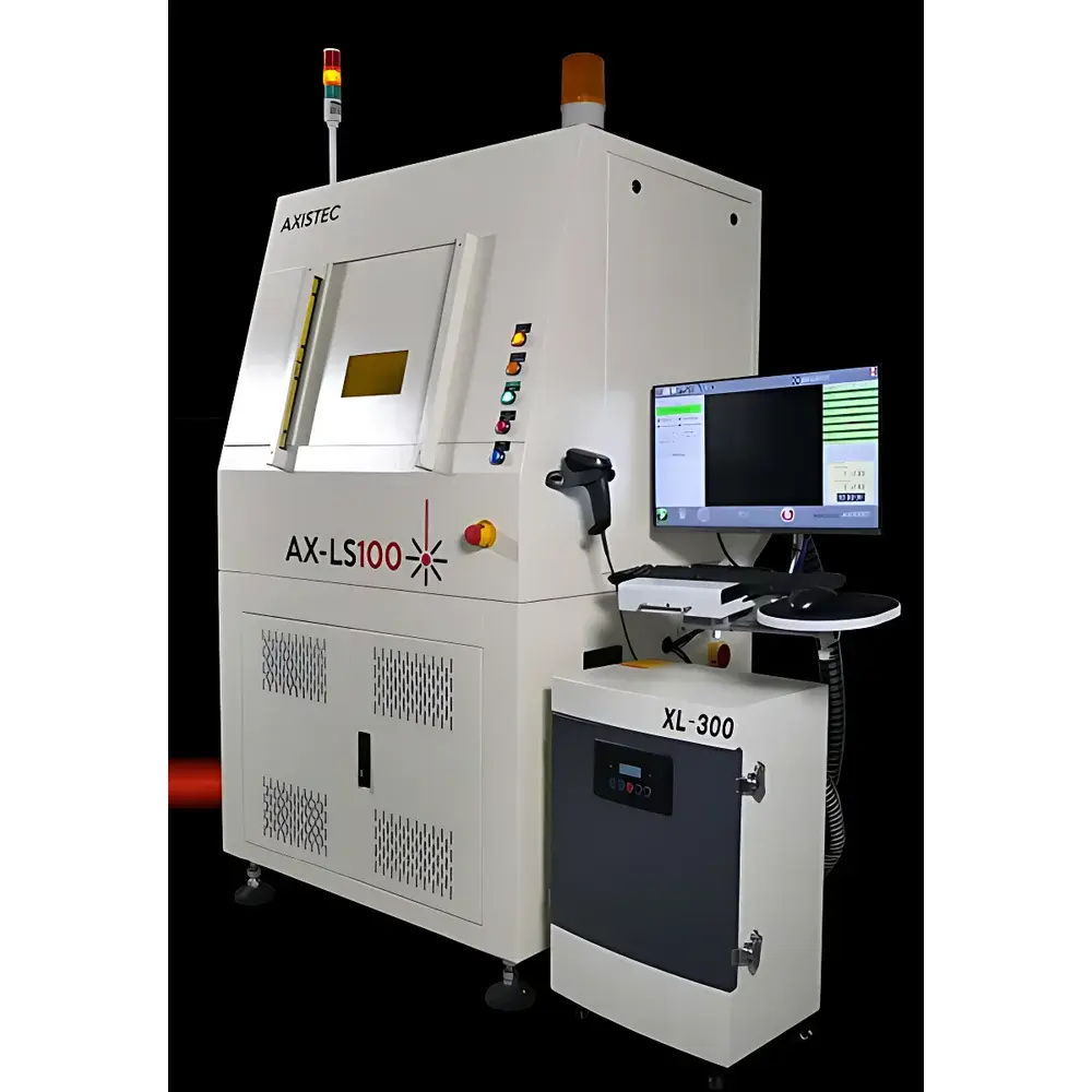
AXIS-TEC AX-LS100 Laser Wafer Dicing System
| Brand | AXIS-TEC |
|---|---|
| Origin | Singapore |
| Manufacturer Type | Authorized Distributor |
| Product Origin | Imported |
| Model | AX-LS100 |
| Maximum Linear Cutting Speed | 800 mm/s |
| Application Scope | Semiconductor Wafer Dicing |
| Maximum Wafer Size | 300 mm (12-inch) |
| Laser Class | Class 1 Enclosure |
| Dimensions (W×L×H) | 1530 × 900 × 2229 mm |
| Weight | 750 kg |
Overview
The AXIS-TEC AX-LS100 Laser Wafer Dicing System is a high-precision, industrial-grade semiconductor dicing platform engineered for non-contact, thermal stress-induced scribing and stealth dicing of silicon, SiC, GaN, and other compound semiconductor wafers. Unlike mechanical dicing saws that rely on abrasive diamond blades and generate kerf loss, mechanical chipping, and subsurface damage, the AX-LS100 employs a pulsed near-infrared (NIR) laser source focused beneath the wafer surface to induce controlled micro-crack propagation along predefined paths. This process—commonly referred to as “stealth dicing”—enables clean, narrow kerf (35–50 µm), minimal thermal influence zone (HAZ), and exceptional edge integrity without post-cut cleaning or etching. Designed for front-side and back-side dicing applications in advanced packaging (e.g., Fan-Out WLP, TSV, chiplets), the system delivers repeatable sub-micron positional accuracy and supports full automation integration in ISO Class 5–7 cleanroom environments.
Key Features
- Class 1 fully enclosed laser workstation with interlocked safety architecture compliant with IEC 60825-1 and ANSI Z136.1 standards
- Automated wafer alignment system with integrated vision-based pattern recognition and sub-pixel centroid detection for ±0.5 µm registration repeatability
- High-dynamic-range XYZ translation stage with air-bearing linear motors, achieving <±50 nm bidirectional positioning accuracy and 800 mm/s maximum scan velocity
- Intuitive touchscreen HMI with recipe-driven operation, real-time laser power monitoring, and parameter logging per die lot
- Modular laser head with integrated height compensation sensor (±150 µm range), enabling automatic focus adjustment across wafer thickness variations (50–1000 µm)
- Optional SECS/GEM interface compliant with SEMI E30/E37 standards for factory-wide equipment connectivity, traceability, and SPC data export
Sample Compatibility & Compliance
The AX-LS100 accommodates standard semiconductor wafers up to 300 mm in diameter and thicknesses ranging from 50 µm (thinned Si) to 1000 µm (bulk GaAs). It supports both bare and tape-mounted wafers on standard FOUPs or open cassettes. The system meets critical regulatory requirements for semiconductor manufacturing infrastructure, including ISO 14644-1 (cleanroom classification), SEMI S2/S8 (safety and ergonomics), and EU Machinery Directive 2006/42/EC. When configured with nitrogen purge, it satisfies inert-atmosphere processing specifications outlined in JEDEC JEP122G for moisture-sensitive devices and enables compliance with internal fab yield control protocols requiring low-particulate, oxidation-free scribe lines.
Software & Data Management
Controlled by AXIS-TEC’s proprietary DICE-OS v4.x software suite, the AX-LS100 provides full audit trail functionality aligned with FDA 21 CFR Part 11 and GLP/GMP documentation standards. All operational parameters—including laser pulse energy, repetition rate, focal depth, scan speed, and gas flow—are timestamped, user-authorized, and stored in encrypted SQLite databases with configurable retention policies. The software supports multi-level access control (operator, engineer, administrator), electronic signature capture for critical parameter changes, and automated report generation (PDF/CSV) for process qualification (PQ), installation qualification (IQ), and operational qualification (OQ) documentation. Optional integration with MES via SECS/GEM allows real-time dispatching of dicing recipes, collection of cycle time metrics, and alarm forwarding to central SCADA systems.
Applications
- Stealth dicing of silicon and wide-bandgap substrates (SiC, GaN, InP) for power electronics and RF devices
- Low-damage scribing prior to cleaving of optoelectronic wafers (LEDs, VCSELs, photodetectors)
- Front-side dicing of ultra-thin wafers (<100 µm) where blade chipping risk exceeds acceptable yield thresholds
- Back-grinding compatible dicing for TSV and 3D-IC stacking processes
- Chip-scale packaging (CSP) and fan-out wafer-level packaging (FOWLP) singulation with minimal die warpage
- R&D prototyping of heterogeneous integration platforms requiring selective material ablation and minimal HAZ
FAQ
What laser wavelength and pulse duration does the AX-LS100 use?
The system utilizes a Q-switched Nd:YAG or fiber laser operating at 1064 nm with pulse durations in the nanosecond regime (typically 10–100 ns), optimized for nonlinear absorption and subsurface modification in crystalline semiconductors.
Is the AX-LS100 compatible with existing cleanroom AMHS interfaces?
Yes—when equipped with the optional auto-loader module and SECS/GEM interface, the system supports standard FOUP handling protocols (SEMI E47.1) and integrates with major AMHS vendors including Brooks, Muratec, and Daifuku.
How is laser focus maintained across warped or bowed wafers?
The integrated capacitive height sensor continuously measures Z-offset during stage motion and dynamically adjusts objective lens position via closed-loop piezo actuation, ensuring consistent focal plane alignment within ±0.3 µm tolerance.
Does the system support process validation documentation for ISO 9001 or IATF 16949 audits?
Yes—the DICE-OS software includes built-in IQ/OQ/PQ templates, calibration log tracking, and revision-controlled recipe management, all exportable in formats accepted by third-party auditors.
Can the AX-LS100 perform partial-depth scribing for subsequent breakage or tape expansion?
Yes—depth-controlled scribing mode allows precise modulation of laser energy and scan passes to achieve programmable crack depth (e.g., 20–80% of wafer thickness), enabling controlled separation via tape expansion or mechanical breaking.


