Bestron INSTEMS MET/MT/ME/ET/M Series In Situ Atomic-Scale Dual-Axis Tilt TEM Holder with Integrated Force–Thermal–Electrical Stimuli
| Brand | Bestron |
|---|---|
| Origin | Beijing, China |
| Manufacturer Type | Authorized Distributor |
| Product Category | Domestic |
| Model | INSTEMS MET/MT/ME/ET/M |
| Application Field | Materials Science |
| Instrument Classification | In Situ Tensile/Compression/Bending Holder |
| Thermal Range | RT–1200 °C |
| Max Force Output | >100 mN |
| Max Displacement | >4 µm |
| Minimum Step Resolution | <0.5 nm |
| Dual-Tilt Range (α/β) | ±25° each |
| Tilt Precision | <0.1° |
| Thermal Ramp Rate | >10,000 °C/s |
| Temperature Accuracy | ≥98% |
| Thermometry Method | Four-Probe Resistive |
| EDS Compatibility | Yes |
| Electrical Output | ±50 V |
| Current Measurement Range | 1 pA–1 A |
| Voltage Measurement Range | 100 nV–50 V |
| Spatial Resolution (in situ) | ≤0.1 nm |
| Drift Stability | <50 pm/s |
Overview
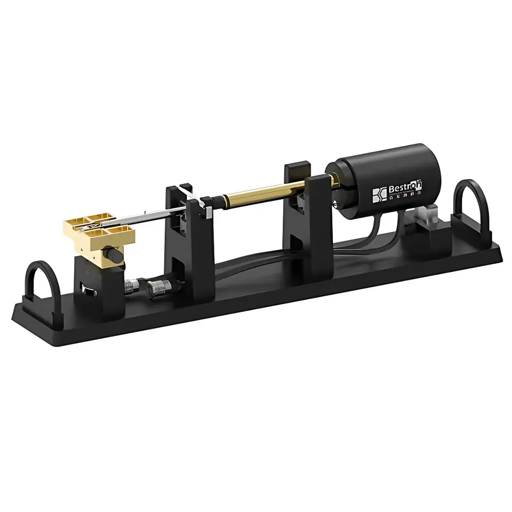
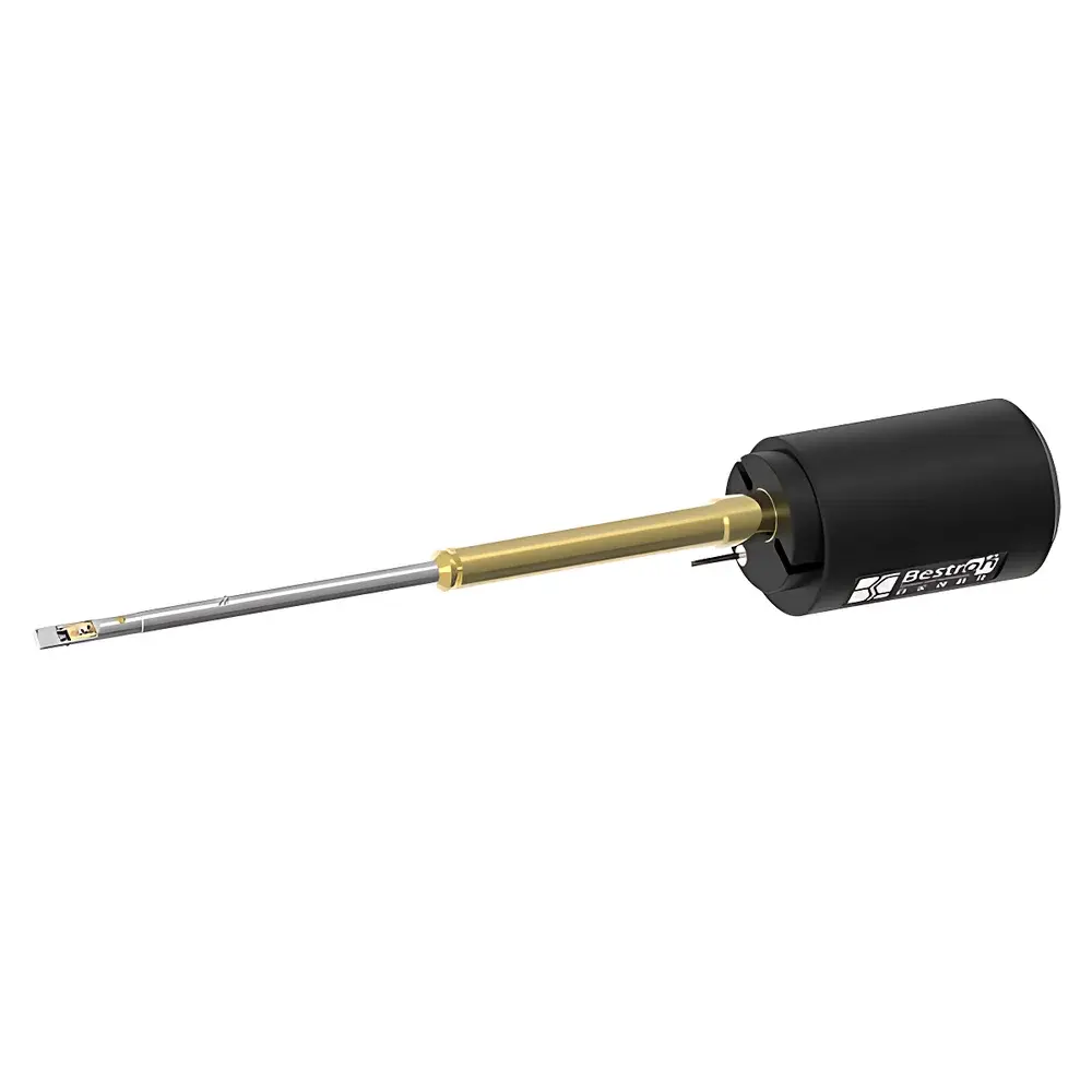
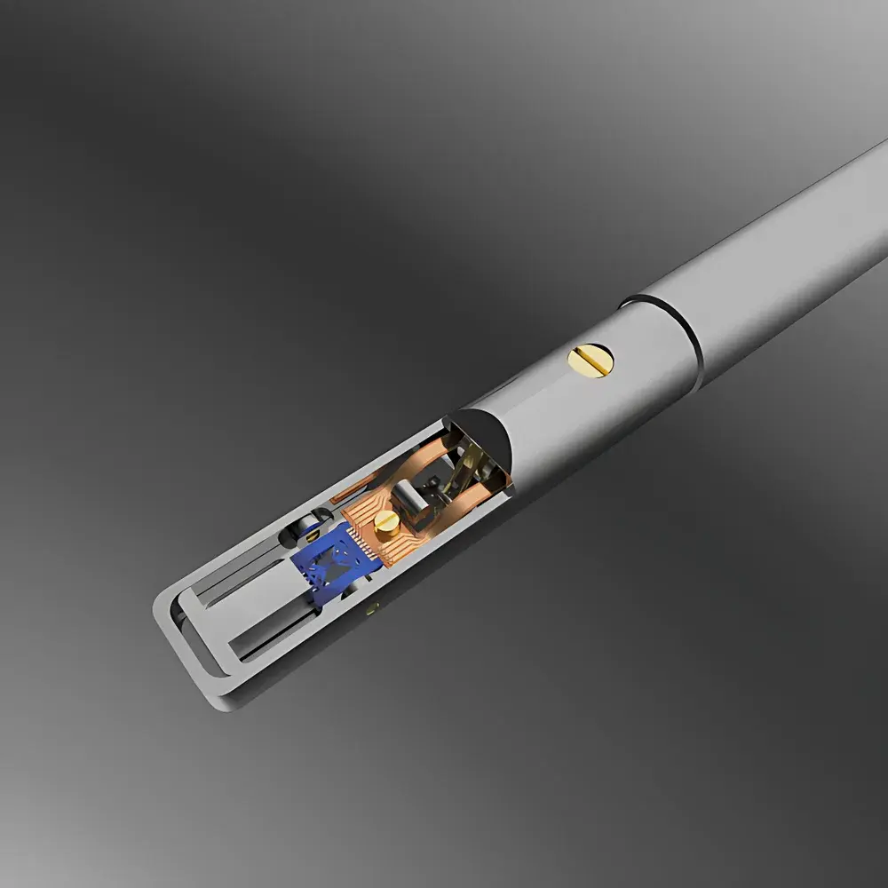
The Bestron INSTEMS MET/MT/ME/ET/M Series is a high-integration, MEMS-based in situ transmission electron microscopy (TEM) sample holder engineered for simultaneous atomic-resolution imaging and multi-field stimuli application under controlled mechanical, thermal, and electrical loading. Unlike conventional probe-type in situ holders limited to single-axis tilt and unidirectional force application, the INSTEMS platform implements orthogonal dual-axis tilt (α and β, each ±25°) within the confined TEM specimen chamber—enabling crystallographically aligned viewing of dynamic structural evolution across multiple zone axes during coupled stimuli. Its core architecture integrates a custom-designed silicon-on-insulator (SOI) MEMS chip with monolithic piezoelectric microactuators and four-terminal sensing electrodes, ensuring decoupled, sub-nanometer mechanical actuation, rapid resistive heating (up to 1200 °C), and picoampere-level current measurement—all while preserving the microscope’s native point resolution (<0.1 nm) and minimizing thermal drift (<50 pm/s). The system operates on fundamental principles of solid-state thermomechanics and electro-thermo-mechanical coupling, making it suitable for quantitative structure–property–process correlation in advanced functional and structural materials.
Key Features
- Dual-axis orthogonal tilt mechanism enabling crystallographic reorientation during multi-field stimulation without compromising TEM alignment or resolution
- MEMS-based miniaturized lab (Mini-lab) platform with interchangeable experimental modules—supporting independent or combinatorial force, thermal, and electrical stimuli
- Four-probe resistive heating and real-time temperature feedback with accuracy ≥98% and ramp rates exceeding 10,000 °C/s
- Piezoelectric microactuator with 100 mN maximum output force, and >4 µm total displacement
- Integrated pA–A current measurement and 100 nV–50 V voltage sourcing via low-noise, galvanically isolated source-measure units (SMUs)
- Full EDS and EELS compatibility; no signal interference from on-chip electronics or thermal gradients
- Robust electromagnetic shielding and mechanical damping design ensures long-term stability and compatibility with JEOL, Thermo Fisher, and Hitachi TEM platforms
Sample Compatibility & Compliance
The INSTEMS holder accommodates bulk foils, nanowires, 2D flakes (e.g., graphene, TMDs), and thin-film heterostructures—regardless of conductivity or magnetic susceptibility—as long as samples are non-ferromagnetic and compatible with standard TEM grid mounting. All Mini-lab variants comply with ISO/IEC 17025 calibration traceability requirements for force and temperature metrology. Electrical subsystems conform to IEC 61000-4-3 (EMC immunity) and UL 61010-1 (electrical safety). Data acquisition meets FDA 21 CFR Part 11 audit-trail requirements when operated with validated software configurations, supporting GLP/GMP-compliant materials qualification workflows in semiconductor and aerospace R&D environments.
Software & Data Management
The proprietary INSTEMS Control Suite provides synchronized, time-stamped control of all three stimulus domains. Mechanical loading modes include monotonic tension/compression, cyclic fatigue, nanoindentation, and bending; thermal protocols support isothermal holds, linear ramps, and step-and-hold sequences; electrical waveforms include DC, pulsed DC, sine, square, triangle, sawtooth, and arbitrary user-defined profiles. All parameters are logged at up to 1 kHz sampling rate and exported in HDF5 format for post-acquisition correlation with TEM image stacks, diffraction patterns, and spectral data. Software supports scripting via Python API for automated experiment sequencing and integration with third-party TEM acquisition platforms (e.g., DigitalMicrograph, Velox).
Applications
- Atomic-scale in situ observation of dislocation nucleation, grain boundary migration, and phase transformation kinetics under thermo-mechanical coupling (e.g., Ni-based superalloys at 1150 °C)
- Real-time tracking of ion migration, interfacial degradation, and electromigration-driven void formation in solid-state batteries and memristive devices
- Quantitative analysis of piezoelectric strain response and domain wall dynamics in ferroelectric oxides under concurrent electric and mechanical fields
- In situ EDS mapping during high-temperature elemental diffusion in high-entropy alloys, correlated with lattice strain evolution measured via geometric phase analysis (GPA)
- Thermoelectric property degradation mechanisms in SnSe and Bi₂Te₃ under thermal–electrical stress, resolved at sub-nanometer scale
FAQ
Is the INSTEMS holder compatible with aberration-corrected TEMs?
Yes—the mechanical and thermal design maintains sub-ångström stability, enabling use with Cs-corrected instruments operating at 80–300 kV without resolution loss.
Can the same Mini-lab module perform force–thermal–electrical tri-field coupling?
No—tri-field coupling requires sequential or paired Mini-lab swaps (e.g., MT + ME); true simultaneous triple-field operation is not supported due to physical and thermal crosstalk constraints.
What is the maximum sample thickness supported?
Standard configuration supports ≤100 nm electron-transparent regions; thicker specimens require focused ion beam (FIB) thinning prior to loading.
Does the system support in situ heating during STEM mode?
Yes—compatible with both parallel-beam TEM and scanning TEM (STEM) configurations, including annular dark-field (ADF) and differential phase contrast (DPC) imaging.
Are calibration certificates provided for force and temperature sensors?
Each unit ships with NIST-traceable calibration reports for thermal sensors and certified load-cell verification data per ISO 376, valid for 12 months from shipment.


