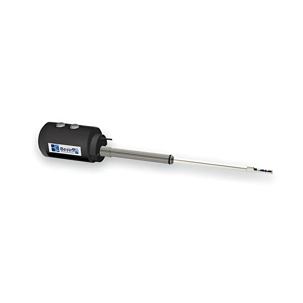
Bestron INSTEMS-M In Situ Dual-Axis Tilt Nanomechanical Testing System for Transmission Electron Microscopy
| Brand | Bestron |
|---|---|
| Model | INSTEMS-M |
| Type | MEMS-Based In Situ TEM Mechanical Testing Holder |
| Loading Modes | Tension, Compression, Nanoindentation, Bending, Impact, Creep, Fatigue |
| Force Range | >100 mN |
| Displacement Range | 4 µm |
| Actuation Resolution | <500 pm |
| Drift Rate | <50 pm/s |
| Spatial Resolution (TEM-compatible) | ≤0.1 nm |
| Dual-Axis Tilt | α ±20°, β ±10° |
| Compatibility | Standard 3-mm TEM specimen holders, Gatan/FEI/Thermo Fisher-compatible apertures |
| Chip Customization | User-configurable MEMS chip geometry and loading configuration |
Overview
The Bestron INSTEMS-M is a high-precision, dual-axis tilt in situ nanomechanical testing system engineered specifically for integration within transmission electron microscopes (TEM). It enables real-time, atomic-resolution observation of material deformation mechanisms—such as dislocation nucleation and motion, phase transformation, crack initiation, and grain boundary sliding—under controlled mechanical loading. Based on monolithic MEMS (Micro-Electro-Mechanical Systems) architecture, the INSTEMS-M employs piezoelectric actuators co-fabricated with the sample chip to deliver sub-nanometer displacement control parallel to the double-tilt plane. Unlike conventional mechanical or thermal actuation approaches, this design eliminates cross-talk between tilting and loading axes, ensuring stable specimen alignment and minimal image drift (<50 pm/s) during extended acquisition sequences. The system is fully compatible with standard 3-mm TEM holder geometries and supports seamless integration with major commercial TEM platforms—including Thermo Fisher Scientific (Titan, Talos), JEOL (ARM, GRAND ARM), and Hitachi (HT7800)—without requiring modifications to column hardware or vacuum interlocks.
Key Features
- Dual-Axis Independent Tilt Control: Precision goniometric rotation with α-axis tilt up to ±20° and β-axis tilt up to ±10°, enabling crystallographic zone-axis alignment and optimal diffraction contrast prior to and during mechanical testing.
- Nanomechanical Actuation with Sub-Picometer Resolution: Piezoelectric-driven displacement with <500 pm actuation precision and 4 µm total stroke; force output exceeds 100 mN, supporting quantitative nano-tensile, nano-compression, nano-indentation, bending, impact, creep, and fatigue experiments.
- MEMS Chip Flexibility: Interchangeable and customizable silicon-based MEMS chips allow adaptation to diverse specimen geometries (e.g., nanopillars, thin films, nanowires) and loading configurations (uniaxial tension, four-point bending, wedge indentation).
- Atomic-Scale Imaging Stability: Optimized thermal and mechanical decoupling ensures TEM imaging stability at ≤0.1 nm spatial resolution under active loading—critical for capturing dynamic lattice-scale phenomena via HRTEM, STEM, or 4D-STEM.
- Vacuum & Electrical Interface Compliance: Fully UHV-compatible (≤1×10⁻⁷ Pa operating pressure); includes feedthroughs for synchronized electrical biasing (optional add-on) and real-time load/displacement feedback via integrated strain gauges or capacitive sensors.
Sample Compatibility & Compliance
The INSTEMS-M accommodates specimens ranging from freestanding nanowires (diameter ≥50 nm) to focused-ion-beam (FIB)-prepared lamellae (thickness ≤100 nm) and sputter-deposited thin films. Its MEMS chip architecture supports both lift-out and in-situ growth-compatible configurations. All materials and surface treatments comply with ISO 14644-1 Class 5 cleanroom handling standards. The system meets mechanical safety requirements per ISO 12100 and electromagnetic compatibility per IEC 61326-1. For regulated environments, the optional data acquisition module supports audit-trail logging aligned with FDA 21 CFR Part 11 principles when used with validated third-party software.
Software & Data Management
The INSTEMS-M operates via a dedicated LabVIEW-based control interface that synchronizes mechanical actuation, tilt positioning, and external TEM signal acquisition (e.g., diffraction pattern streaming, EELS spectrum imaging). Load–displacement curves are time-stamped and exported in HDF5 format for interoperability with Python-based analysis pipelines (e.g., HyperSpy, Atomap). Real-time drift correction algorithms integrate with DigitalMicrograph™ plugins, while batch experiment scripting supports automated cyclic loading protocols with configurable dwell times, ramp rates, and trigger conditions. All experimental metadata—including tilt angles, applied force, temperature (if coupled with INSTEMS-T), and camera parameters—is embedded in FAIR-compliant headers.
Applications
This system is routinely deployed in advanced materials research laboratories to investigate fundamental deformation physics in metallic nanostructures (e.g., high-strength steel nanowires, Al–Mg alloys, Ti–6Al–4V thin films), ceramic composites, 2D materials (MoS₂, graphene heterostructures), and battery electrode interfaces (Si anodes, NMC cathodes). It supports structure–property correlation studies required for ASTM E2627 (standard guide for in situ mechanical testing in electron microscopes) and contributes directly to GLP-compliant failure analysis workflows in aerospace and nuclear materials qualification.
FAQ
Is the INSTEMS-M compatible with aberration-corrected TEMs?
Yes—it maintains mechanical and thermal stability under the stringent vibration and drift requirements of Cs-corrected instruments operating at 80–300 kV accelerating voltages.
Can I perform simultaneous EDS or EELS during mechanical loading?
Yes—integrated electrical feedthroughs support concurrent spectroscopic acquisition without signal interference; beam-induced charging is mitigated via low-energy electron flood gun synchronization.
What is the lead time for custom MEMS chip fabrication?
Standard chips ship within 6–8 weeks; complex multi-layer or high-aspect-ratio designs require 12–14 weeks, subject to design review and process validation.
Does the system support closed-loop force control?
Yes—capacitive displacement sensing combined with piezo voltage feedback enables real-time PID-regulated force control with bandwidth up to 100 Hz.
Are training and installation services included?
Comprehensive on-site installation, TEM integration validation, and operator certification are available as optional service packages, aligned with ISO/IEC 17025 competency guidelines.


