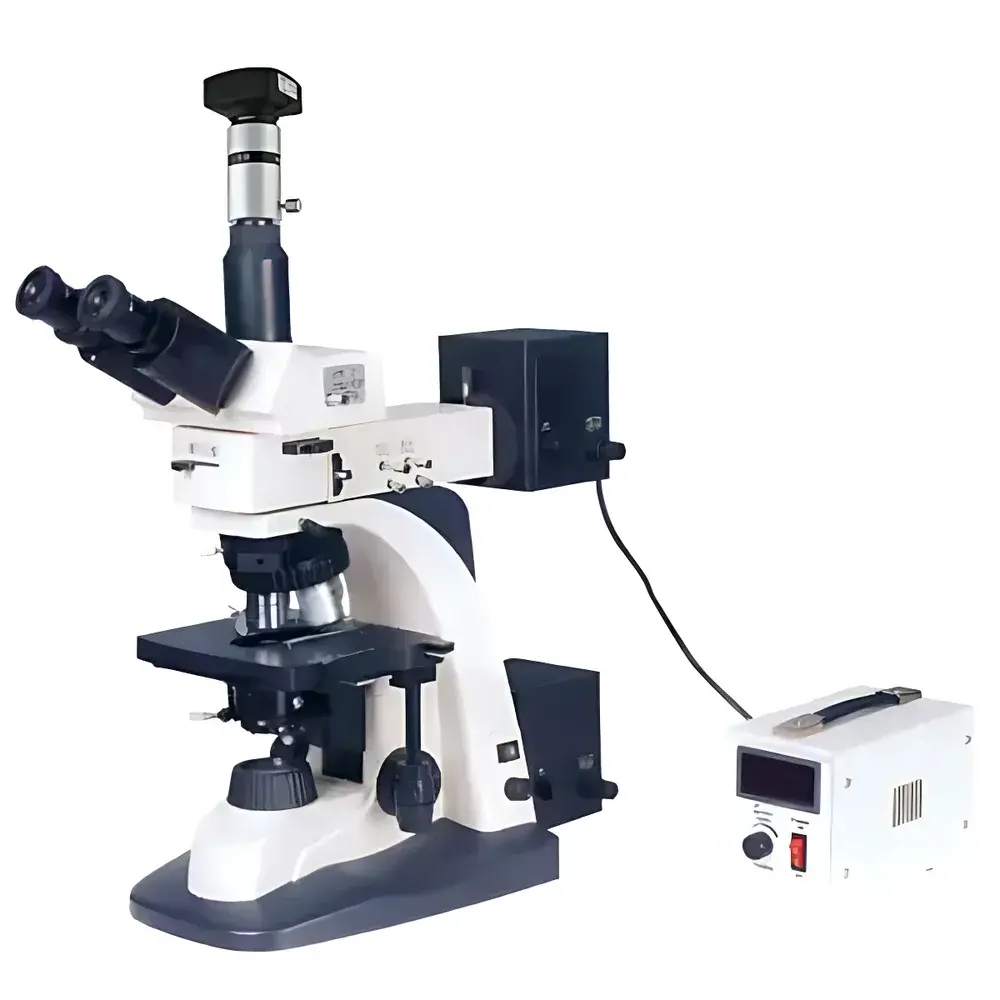
BM-SG20BD D Advanced Upright Metallurgical Microscope
| Brand | BM (Biaimu) |
|---|---|
| Origin | Shanghai, China |
| Model | BM-SG20BD D |
| Illumination | Reflected (Epi-illumination) & Transmitted |
| Optical Design | Infinity-Corrected, Dual-Path (Brightfield/Darkfield/DIC/Polarized) |
| Eyepiece Tube | 30° Inclined Trinocular |
| Objective Turret | Quadruple with DIC Slot |
| Total Magnification Range | 50×–500× (with 10× eyepieces and standard objectives) |
| Eyepieces | Widefield Plan 10×/25 mm, Crosshair 10×/20 mm (0.1 mm graticule) |
| Objectives | Infinity-Corrected Long Working Distance Plan Apochromat BF/DF, 5×/0.10, 10×/0.25, 20×/0.40, 50×/0.55 |
| Condenser | NA 1.25 Abbe with Iris Diaphragm & Filter Holder |
| Focus Mechanism | Coaxial Coarse/Fine Drive, Fine Adjustment Graduation: 2 µm |
| Stage | Dual-layer Mechanical Stage, 189 × 160 mm, Travel: 80 × 50 mm |
| Polarization System | Rotatable Analyzer (0–360°), Removable Polarizer & Analyzer |
| Illumination Sources | 12 V/50 W Halogen (Reflected & Transmitted), Kӧhler Illumination, Continuous Intensity Control, Field & Aperture Diaphragms |
| Camera Interface | GT5.0 5 MP CMOS Sensor with MCL-Z C-mount Adapter |
| Software | Geometric Metrology Suite (Point, Line, Circle, Arc, Straightness, Roundness, Area) |
Overview
The BM-SG20BD D Advanced Upright Metallurgical Microscope is an infinity-corrected, dual-illumination optical system engineered for high-fidelity microstructural analysis of opaque and reflective specimens. Designed in accordance with ISO 10934-1 (Microscopy — Nomenclature of components of light microscopes) and aligned with ASTM E3-22 (Standard Guide for Preparation of Metallographic Specimens), it supports quantitative metallurgical evaluation across semiconductor wafers, electronic packaging substrates, precision die-cast alloys, sintered ceramics, and heat-treated tool steels. Its modular architecture integrates epi-illumination for reflected-light observation (brightfield, darkfield, differential interference contrast [DIC], and polarized light) with transmitted-light Köhler illumination for transparent or semi-transparent reference standards or thin-sectioned intermetallics. The 200 mm focal length tube lens ensures chromatic fidelity across the full visible spectrum (400–700 nm), while the long-working-distance plan apochromat objectives minimize parallax and enable safe imaging of topographically complex surfaces—critical for failure analysis labs conducting cross-sectional inspection of solder joints or thermal barrier coatings.
Key Features
- Infinity-corrected optical path with f = 200 mm tube lens, enabling stable beam collimation and compatibility with auxiliary modules (e.g., DIC prisms, polarization rotators, fluorescence filters)
- Quadruple objective turret with dedicated DIC slot and precise mechanical indexing—ensuring repeatable alignment for quantitative birefringence or stress-induced contrast measurements
- 30° inclined trinocular head with 100:0 / 0:100 beam-splitting ratio, supporting simultaneous visual observation and digital acquisition without optical degradation
- Long working distance (LWD) plan apochromat objectives (5× to 50×) optimized for both brightfield and darkfield illumination—NA values range from 0.10 to 0.55, delivering high resolution (≤0.7 µm at 50×) and depth-of-field consistency across magnifications
- Coaxial coarse/fine focusing mechanism with 2 µm fine-adjustment graduation and ergonomic torque control—designed for extended-focus stacking and precise Z-axis metrology
- Rotatable analyzer (0–360°) with calibrated angular scale and removable polarizer/analyzer modules—enabling quantitative crystallographic orientation mapping per ASTM E112 and ISO 643
- Dual halogen illumination system (12 V/50 W): independent reflected and transmitted paths, each equipped with field and aperture diaphragms, intensity regulators, and color filter holders (green, blue, neutral density)
Sample Compatibility & Compliance
The BM-SG20BD D accommodates specimens up to 30 mm in height and 100 mm in diameter on its dual-layer mechanical stage (189 × 160 mm, 80 × 50 mm travel). It supports polished metallographic mounts, wafer fragments, PCB cross-sections, powder metallurgy compacts, and ceramic fracture surfaces. All optical components comply with ISO 8578 (Microscopy — Specification of image quality for objective lenses) and are certified for use in GLP-regulated environments. The microscope’s illumination stability (< ±2% intensity drift over 4 hours) and reproducible focus repeatability (±0.5 µm over 100 cycles) meet internal validation requirements for QC laboratories operating under ISO/IEC 17025. Optional oil-immersion objectives (100×, NA 1.25) extend analytical capability to sub-micron grain boundary delineation in austenitic stainless steels per ASTM E112 Annex A3.
Software & Data Management
The integrated GT5.0 5 MP CMOS camera connects via USB 3.0 and interfaces with a metrology-grade software suite compliant with FDA 21 CFR Part 11 requirements (audit trail, electronic signature, user access levels). Measurement functions include calibrated point-to-point distance, chord-length arc analysis, circularity deviation (per ISO 1101), area fraction quantification (e.g., porosity in aluminum castings per ASTM E1245), and straightness evaluation of machined edges. Raw image metadata (magnification, objective ID, exposure time, timestamp) is embedded in TIFF headers. Export formats include CSV (for statistical process control integration), PDF reports with annotated overlays, and DICOM-compatible stacks for multi-plane reconstruction. All calibration files are traceable to NIST-traceable stage micrometers (0.01 mm division).
Applications
- Semiconductor process control: Defect identification on Si wafers (scratches, pits, particle contamination) using darkfield and DIC contrast enhancement
- Electronic packaging: Solder joint integrity assessment (void fraction, intermetallic layer thickness) in QFN and BGA assemblies
- Metallurgical QA/QC: Grain size distribution analysis (ASTM E112), inclusion rating (ASTM E45), and phase quantification (ferrite/austenite in duplex steels)
- Precision tooling: Hardness indentation geometry verification (Vickers/Knoop) and crack propagation path mapping in HSS end mills
- Advanced ceramics: Pore network characterization in Y-TZP zirconia implants and thermal spray coatings
- Failure analysis: Fractography of fatigue striations, cleavage facets, and ductile dimples in aerospace titanium alloys (ASTM E338)
FAQ
What is the maximum specimen height supported by the stage?
The vertical clearance between the top of the stage and the bottom of the lowest objective (5×) is 30 mm—sufficient for standard metallographic mounts and wafer edge chips.
Is the microscope compatible with third-party image analysis platforms such as ImageJ or Olympus cellSens?
Yes—the GT5.0 camera outputs standard UVC-compliant video streams; drivers and SDKs are provided for custom integration with MATLAB, Python OpenCV, or commercial packages.
Can the polarization module be used for quantitative birefringence measurement?
The 360° calibrated analyzer enables relative retardation estimation using Michel-Levy charts; for absolute retardation, optional compensators (e.g., quartz wedge) may be inserted into the intermediate tube.
Does the system support automated focus mapping for rough or tilted samples?
While the BM-SG20BD D does not include motorized Z-drive, its fine-focus graduation (2 µm) and stage verniers allow manual focus stacking; external motorized Z-stages can be retrofitted via standard M42 mounting threads.
Are calibration certificates available for the stage micrometer and camera pixel scale?
NIST-traceable calibration documentation is supplied with each instrument shipment, including uncertainty budgets per ISO/IEC 17025 Annex A.


